Why is Via Filling Important?
Via filling plays a crucial role in the functionality and durability of multi-layer PCBs. Some of the key reasons why via filling is important include:
-
Electrical Continuity: Via filling ensures that there is a reliable electrical connection between the different layers of a PCB. This is essential for the proper functioning of the electronic components mounted on the board.
-
Mechanical Strength: Filled vias provide additional mechanical strength to the PCB, making it more resistant to stress and vibration. This is particularly important for PCBs used in high-stress environments, such as automotive or aerospace applications.
-
Thermal Management: Filled vias can also act as thermal conduits, helping to dissipate heat from high-power components on the PCB. This can prevent overheating and extend the lifespan of the electronic components.
-
Signal Integrity: Via filling can help to minimize signal reflections and crosstalk, which can degrade the quality of high-speed signals transmitted through the PCB.
Via Filling Materials
There are several materials that can be used for via filling, each with its own advantages and disadvantages. Some of the most common via filling materials include:
-
Conductive Epoxy: Conductive epoxy is a popular choice for via filling due to its ease of application and good electrical conductivity. It is a mixture of epoxy resin and conductive particles, such as silver or copper.
-
Copper Plating: Copper plating involves depositing a layer of copper inside the via using an electroplating process. This method provides excellent electrical conductivity and mechanical strength but can be more expensive and time-consuming than other methods.
-
Solder Paste: Solder paste can be used to fill vias, especially in cases where the PCB will undergo a subsequent Reflow Soldering process. This method is relatively simple and inexpensive but may not provide the same level of reliability as other methods.
| Material | Advantages | Disadvantages |
|---|---|---|
| Conductive Epoxy | Easy to apply, good electrical conductivity | Lower conductivity than metal fillings |
| Copper Plating | Excellent conductivity and strength | More expensive and time-consuming |
| Solder Paste | Simple and inexpensive | May not provide the same level of reliability |
Via Filling Techniques
There are several techniques used for via filling, depending on the material being used and the specific requirements of the PCB. Some of the most common via filling techniques include:
Screen Printing
Screen printing is a popular method for applying conductive epoxy to fill vias. In this process, a stencil is placed over the PCB, and the conductive epoxy is spread over the stencil using a squeegee. The epoxy fills the vias and any excess material is removed. This method is relatively simple and can be used for high-volume production.
Vacuum Filling
Vacuum filling is another method used for applying conductive epoxy or solder paste to fill vias. In this process, the PCB is placed in a vacuum chamber, and the filling material is dispensed onto the surface of the board. The vacuum helps to draw the material into the vias, ensuring complete filling. This method is more precise than screen printing and can be used for smaller vias.
Electroplating
Electroplating is used for copper-filled vias. In this process, the PCB is immersed in a copper plating solution, and an electric current is applied. The copper ions in the solution are attracted to the walls of the vias, forming a thick, conductive layer. This method provides excellent electrical conductivity and mechanical strength but is more expensive and time-consuming than other methods.
Comparison of Via Filling Techniques
| Technique | Suitable Materials | Advantages | Disadvantages |
|---|---|---|---|
| Screen Printing | Conductive Epoxy | Simple, high-volume production | Less precise than other methods |
| Vacuum Filling | Epoxy, Solder Paste | Precise, suitable for small vias | Slower than screen printing |
| Electroplating | Copper | Excellent conductivity and strength | Expensive and time-consuming |

Factors Affecting Via Filling Quality
Several factors can affect the quality of via filling, including:
-
Via Size and Aspect Ratio: Smaller vias and those with higher aspect ratios (depth to width ratio) can be more challenging to fill completely.
-
Material Properties: The viscosity, particle size, and other properties of the filling material can impact the ease and quality of via filling.
-
PCB Design: The layout and density of vias on the PCB can affect the filling process. Closely spaced vias may require special consideration.
-
Process Parameters: The specific parameters used during the filling process, such as temperature, pressure, and fill time, can all impact the quality of the final result.
Testing and Inspection
After via filling, it is important to test and inspect the PCB to ensure that the vias have been filled correctly and that there are no defects that could impact the performance or reliability of the board. Some common testing and inspection methods include:
-
Visual Inspection: A simple visual inspection can reveal any obvious defects, such as incomplete filling or excessive filling material on the surface of the PCB.
-
X-Ray Inspection: X-ray imaging can be used to inspect the internal structure of the filled vias, revealing any voids or other defects that may not be visible from the surface.
-
Electrical Testing: Electrical continuity and resistance testing can be used to verify that the filled vias are providing the expected electrical performance.
-
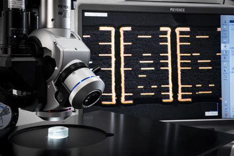
Microsectioning: In some cases, destructive testing may be necessary to fully evaluate the quality of the via filling. Microsectioning involves cutting the PCB and examining the cross-section of the filled vias under a microscope.
Challenges and Limitations
While via filling is an essential process for multi-layer PCBs, there are some challenges and limitations to consider:
-
Cost: Via filling can add significant cost to the PCB manufacturing process, especially for high-density boards with many vias.
-
Process Complexity: Via filling requires specialized equipment and expertise, which can make it more complex and time-consuming than other PCB manufacturing processes.
-
Material Compatibility: Not all PCB materials are compatible with all via filling materials. It is important to select materials that are compatible to ensure reliable performance.
-
Size Limitations: Very small vias or those with high aspect ratios can be challenging to fill completely, which may limit the design options for some PCBs.
Future Trends
As electronic devices continue to become smaller and more complex, the demand for high-density PCBs with reliable via filling is expected to grow. Some of the future trends in via filling technology include:
-
Advanced Materials: The development of new, high-performance filling materials with improved electrical and thermal properties.
-
Automated Processes: Increased automation of via filling processes to improve efficiency and reduce costs.
-
3D Printing: The use of 3D printing technologies to create PCBs with filled vias, potentially reducing the need for traditional via filling processes.
-
Embedded Components: The integration of passive components, such as capacitors and resistors, into the PCB Substrate, which may require new via filling techniques.
Frequently Asked Questions (FAQ)
- What is the difference between via filling and via plating?
-
Via filling involves completely filling the via with a conductive material, while via plating involves coating the walls of the via with a conductive layer, typically copper. Via filling provides better electrical and thermal conductivity, as well as improved mechanical strength.
-
Can all PCBs benefit from via filling?
-
While via filling is essential for multi-layer PCBs, not all PCBs require via filling. Single-layer or double-layer PCBs with large vias may not benefit significantly from via filling. The decision to use via filling depends on the specific requirements of the PCB design and application.
-
How does via filling affect the manufacturing time and cost of PCBs?
-
Via filling can add significant time and cost to the PCB manufacturing process, especially for high-density boards with many vias. The specific impact depends on the via filling method used, the number and size of the vias, and the material costs.
-
What are the most common defects in via filling, and how can they be prevented?
-
Common defects in via filling include incomplete filling, voids, and excessive filling material on the surface of the PCB. These defects can be prevented by carefully controlling the filling process parameters, selecting compatible materials, and performing adequate testing and inspection.
-
Can via filling be used for Flexible PCBs?
- Yes, via filling can be used for flexible PCBs, but the choice of filling material and process may differ from rigid PCBs. Conductive epoxies and solder pastes are commonly used for filling vias in flexible PCBs, as they can withstand the bending and flexing of the board.
Conclusion
Via filling is a critical process in the manufacturing of multi-layer PCBs, ensuring electrical continuity, mechanical strength, thermal management, and signal integrity. The choice of via filling material and technique depends on the specific requirements of the PCB design and application, as well as cost and performance considerations.
As electronic devices continue to advance, the demand for reliable and high-performance via filling solutions is expected to grow. Innovations in materials, processes, and technologies will play a key role in meeting these demands and enabling the development of next-generation electronic products.
By understanding the importance of via filling, the various materials and techniques available, and the factors affecting via filling quality, PCB designers and manufacturers can make informed decisions to ensure the optimal performance and reliability of their products.
Leave a Reply