Understanding High-Speed Signals
What Are High-Speed Signals?
High-speed signals are electrical signals that have high frequencies and fast rise and fall times. These signals are typically used in applications such as high-speed digital circuits, high-bandwidth analog circuits, and radio frequency (RF) systems. The frequency range for high-speed signals can vary depending on the application, but it generally starts at around 100 MHz and can go up to several gigahertz (GHz).
Characteristics of High-Speed Signals
High-speed signals have several unique characteristics that distinguish them from low-speed signals:
-
Fast rise and fall times: High-speed signals have very short transition times between logic states, which can be in the order of picoseconds (ps) or nanoseconds (ns).
-
High frequencies: The frequency of high-speed signals is typically much higher than that of low-speed signals, often in the range of hundreds of megahertz (MHz) to several gigahertz (GHz).
-
Transmission line effects: At high frequencies, the PCB traces behave like transmission lines, which means that the signals are subject to effects such as impedance mismatch, reflections, and crosstalk.
-
Sensitivity to noise: High-speed signals are more susceptible to noise and interference than low-speed signals, which can lead to signal integrity issues and data corruption.
Challenges in High-Speed PCB Design
Designing high-speed PCBs presents several challenges that must be addressed to ensure optimal performance and reliability.
Signal Integrity
Signal integrity is a major concern in high-speed PCB Design. As the signal frequency increases, the PCB traces become more susceptible to various signal integrity issues, such as:
-
Reflections: When a signal encounters an impedance mismatch, a portion of the signal is reflected back to the source, causing distortion and signal degradation.
-
Crosstalk: Crosstalk occurs when a signal on one trace induces an unwanted signal on an adjacent trace, leading to interference and noise.
-
Attenuation: As the signal travels through the PCB traces, it experiences attenuation due to resistive, dielectric, and skin effect losses, which can reduce the signal strength and quality.
-
Jitter: Jitter is the deviation of a signal’s timing from its ideal position, which can cause synchronization issues and data errors in high-speed digital systems.
Power Integrity
Power integrity is another critical aspect of high-speed PCB design. As the speed and complexity of electronic devices increase, so does their power consumption. This can lead to various power integrity issues, such as:
-
Voltage drops: When the current drawn by the components exceeds the capacity of the power distribution network (PDN), it can cause voltage drops across the PCB, leading to performance degradation and reliability issues.
-
Ground bounce: Ground bounce occurs when the ground potential fluctuates due to the switching activity of digital circuits, causing noise and signal integrity issues.
-
Electromagnetic interference (EMI): High-speed circuits can generate significant amounts of EMI, which can interfere with other electronic devices and cause compliance issues with electromagnetic compatibility (EMC) regulations.
Thermal Management
High-speed electronic components generate a significant amount of heat, which must be effectively dissipated to ensure reliable operation and prevent thermal damage. Poor thermal management can lead to performance degradation, reduced reliability, and even device failure.
Best Practices for High-Speed PCB Design
To overcome the challenges associated with high-speed PCB design, engineers must follow several best practices and guidelines.
Impedance Control
Impedance control is a critical aspect of high-speed PCB design. To minimize reflections and ensure proper signal propagation, the impedance of the PCB traces must match the impedance of the source and load. This is typically achieved by controlling the trace width, thickness, and spacing, as well as the dielectric properties of the PCB material.
Common impedance-controlled trace geometries include:
- Microstrip: A trace on the outer layer of the PCB, with a ground plane on the layer beneath it.
- Stripline: A trace embedded between two ground planes within the PCB Stackup.
- Coplanar waveguide: A trace on the outer layer of the PCB, with ground planes on either side of the trace.
Routing Techniques
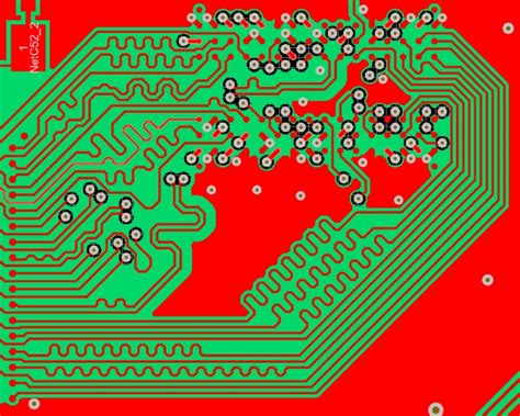
Proper routing techniques are essential for maintaining signal integrity and minimizing crosstalk in high-speed PCB designs. Some key routing guidelines include:
- Keep signal traces as short as possible to minimize losses and delay.
- Avoid sharp bends and corners in traces, as they can cause reflections and impedance discontinuities.
- Use smooth curves and 45-degree angles for trace bends to maintain a consistent impedance profile.
- Maintain a consistent trace width and spacing throughout the signal path to avoid impedance mismatches.
- Avoid routing high-speed signals parallel to each other for long distances to minimize crosstalk.
- Use ground planes and power planes to provide a low-impedance return path for high-speed signals and to minimize EMI.
Decoupling and Filtering
Decoupling and filtering techniques are used to maintain power integrity and reduce noise in high-speed PCB designs. Some common practices include:
- Place decoupling capacitors close to the power pins of high-speed components to provide a local, low-impedance power source and to filter high-frequency noise.
- Use a combination of bulk, ceramic, and tantalum capacitors to provide effective decoupling across a wide frequency range.
- Implement power and ground planes in the PCB stackup to provide a low-impedance power distribution network and to minimize voltage drops.
- Use ferrite beads and common-mode chokes to filter out high-frequency noise and to suppress EMI.
Signal Integrity Simulation
Signal integrity simulation is an essential tool for validating high-speed PCB designs and identifying potential issues before fabrication. Simulation tools can help engineers analyze various aspects of the design, such as:
- Impedance matching and reflections
- Crosstalk and coupling
- Signal attenuation and distortion
- Eye diagrams and jitter analysis
By performing signal integrity simulations, engineers can optimize the design, make necessary adjustments, and ensure that the PCB will perform as expected in the final application.
EMC Considerations
Electromagnetic compatibility (EMC) is a critical consideration in high-speed PCB design. To minimize EMI and ensure compliance with EMC regulations, engineers must follow several guidelines:
- Use proper grounding and shielding techniques to contain high-frequency signals and prevent them from radiating into the environment.
- Implement filter circuits and suppressors to attenuate high-frequency noise and transients.
- Follow PCB layout guidelines for minimizing the loop area of high-speed signals and reducing the coupling between traces.
- Use shielded connectors and cables for high-speed interfaces to prevent EMI from entering or exiting the system.

FAQ
-
What is the difference between high-speed PCB design and regular PCB design?
High-speed PCB design focuses on designing circuits that can handle high-frequency signals and fast data transmission rates, while regular PCB design deals with lower-speed signals and less demanding applications. -
Why is impedance control important in high-speed PCB design?
Impedance control is crucial in high-speed PCB design because it helps minimize reflections and ensures proper signal propagation. By matching the impedance of the PCB traces to the source and load, signal integrity is maintained, and distortion is minimized. -
What are some common signal integrity issues in high-speed PCB design?
Common signal integrity issues in high-speed PCB design include reflections, crosstalk, attenuation, and jitter. These issues can cause signal degradation, noise, and data errors, which can compromise the performance and reliability of the system. -
How can engineers mitigate power integrity issues in high-speed PCB designs?
To mitigate power integrity issues, engineers can use decoupling capacitors, implement power and ground planes, and use filtering techniques such as ferrite beads and common-mode chokes. These practices help maintain a stable power supply and reduce high-frequency noise. -
What is the role of signal integrity simulation in high-speed PCB design?
Signal integrity simulation is used to validate high-speed PCB designs and identify potential issues before fabrication. By analyzing various aspects of the design, such as impedance matching, crosstalk, and signal distortion, engineers can optimize the design and ensure that the PCB will perform as expected in the final application.
Conclusion
High-speed PCB design is a complex and challenging field that requires a deep understanding of signal integrity, power integrity, and EMC principles. As technology continues to advance and the demand for faster, more complex electronic systems grows, the importance of high-speed PCB design will only continue to increase.
By following best practices such as impedance control, proper routing techniques, decoupling and filtering, signal integrity simulation, and EMC considerations, engineers can successfully design high-performance PCBs that meet the demanding requirements of modern electronic applications.
As the world becomes increasingly connected and reliant on high-speed electronic systems, the role of skilled high-speed PCB designers will be more critical than ever in driving innovation and enabling the next generation of cutting-edge technologies.
Leave a Reply