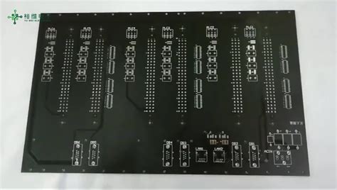
What is a Bare Board?
A bare board, also known as a printed circuit board (PCB) without components, is the foundation of any electronic device. It is a flat, rigid board made of insulating material, typically fiberglass or composite epoxy, with conductive copper traces etched onto its surface. These traces form the electrical connections between the various components that will be mounted on the board later in the manufacturing process.
Bare boards are essential to the functionality and reliability of electronic devices, as they provide the necessary electrical pathways for signals and power to flow between components. The quality of the bare board directly impacts the performance and longevity of the final product.
Types of Bare Boards
There are several types of bare boards, each with its own characteristics and applications:
- Single-sided boards: These boards have copper traces on only one side of the insulating material. They are the simplest and most cost-effective type of bare board, suitable for low-complexity circuits.
- Double-sided boards: These boards have copper traces on both sides of the insulating material, allowing for more complex circuit designs and higher component density. The two sides are connected through plated-through holes (PTHs).
- Multi-layer Boards: These boards consist of multiple layers of insulating material with copper traces on each layer. They offer the highest level of complexity and density, enabling the design of intricate circuits with numerous components. Multi-layer boards are commonly used in advanced electronic devices, such as smartphones, computers, and aerospace systems.
- Flexible boards: These boards are made of flexible insulating material, such as polyimide, allowing them to bend and conform to various shapes. Flexible boards are often used in wearable electronics, medical devices, and applications where space is limited.
The Importance of Bare Board Testing
Bare board testing is a crucial step in the electronics manufacturing process, as it ensures the quality and reliability of the PCB before components are mounted. By detecting and addressing issues at the bare board stage, manufacturers can avoid costly rework and delays later in the production cycle.
Some of the key reasons for conducting bare board testing include:
- Identifying manufacturing defects: Bare board testing can detect various manufacturing defects, such as short circuits, open circuits, incorrect trace widths, and issues with plated-through holes. Identifying these defects early allows for timely correction and prevents defective boards from progressing further in the manufacturing process.
- Ensuring electrical continuity: Testing the electrical continuity of the copper traces on the bare board verifies that the connections between points on the board are intact and meet the specified resistance values. This is essential for the proper functioning of the final product.
- Verifying design integrity: Bare board testing helps validate the PCB design by confirming that the manufactured board matches the intended design. This includes checking the accuracy of trace routing, hole sizes, and spacing between features.
- Improving yield and reducing costs: By identifying and addressing issues at the bare board stage, manufacturers can improve the overall yield of the production process. This translates to reduced material waste, lower rework costs, and faster time-to-market for the final product.
- Meeting quality standards: Bare board testing helps manufacturers meet various quality standards and certifications, such as IPC (Association Connecting Electronics Industries) standards, which are globally recognized benchmarks for PCB manufacturing quality.

Bare Board Testing Methods
There are several methods for testing bare boards, each with its own advantages and limitations. The choice of testing method depends on factors such as the complexity of the board, the required level of coverage, and the available resources.
1. Visual Inspection
Visual inspection is the most basic form of bare board testing, involving a manual examination of the board for visible defects, such as:
- Scratches or damage to the copper traces
- Contamination or foreign material on the board surface
- Incorrect hole sizes or missing holes
- Inconsistent trace widths or spacing
Visual inspection can be performed with the naked eye or using magnification tools, such as microscopes or digital cameras. While visual inspection is relatively quick and inexpensive, it is limited by the inspector’s ability to detect small or hidden defects.
2. Automated Optical Inspection (AOI)
Automated Optical Inspection (AOI) is a computer-based system that uses high-resolution cameras and advanced image processing algorithms to inspect bare boards for defects. AOI systems compare the captured images of the board to a reference image or CAD data, identifying any deviations or anomalies.
Advantages of AOI include:
- High-speed inspection, capable of examining thousands of points on a board in a matter of seconds
- Consistent and repeatable results, eliminating human error and subjectivity
- Ability to detect small defects that may be missed by visual inspection
- Automated data collection and reporting for quality control and traceability
However, AOI systems can be expensive to implement and may require significant programming and setup time for each unique board design.
3. Electrical Testing
Electrical testing involves verifying the electrical continuity and isolation of the copper traces on the bare board. There are two primary methods for electrical testing:
a. Flying Probe Testing: Flying probe testing uses a set of movable probes that make contact with specific points on the board to measure electrical properties, such as resistance, capacitance, and inductance. The probes are controlled by a computer, which positions them according to a predefined test program.
Flying probe testing offers several benefits:
- Flexibility, as the test program can be easily modified for different board designs
- No need for custom fixturing, reducing setup time and costs
- Ability to test both sides of the board simultaneously
- High test coverage, as the probes can access almost any point on the board
However, flying probe testing can be slower than other methods, as the probes must physically move between test points.
b. Fixture-based Testing: Fixture-based testing involves using a custom-designed fixture, also known as a bed-of-nails, which contains an array of spring-loaded pins that make contact with specific points on the board. The fixture is connected to a test system that applies electrical signals and measures the board’s responses.
Advantages of fixture-based testing include:
- High-speed testing, as all test points are contacted simultaneously
- Ability to test multiple boards in parallel, increasing throughput
- Consistent and repeatable contact with the board, ensuring reliable test results
However, fixture-based testing requires the design and fabrication of a custom fixture for each unique board design, which can be time-consuming and expensive.
4. Boundary Scan Testing
Boundary scan testing, also known as JTAG (Joint Test Action Group) testing, is a method for testing the interconnections between integrated circuits (ICs) on a board. It involves using special test circuitry built into the ICs, which allows for the control and observation of the signals at the boundaries of the ICs.
Advantages of boundary scan testing include:
- Ability to test complex boards with high component density
- Access to internal nodes and signals that are not accessible by other testing methods
- Reduced need for physical test points, as the test circuitry is built into the ICs
- Automated test generation and execution, based on the board’s design data
However, boundary scan testing requires the ICs on the board to support the JTAG standard, and it may not provide complete coverage of all interconnections on the board.

Bare Board Testing Standards
Several industry standards govern the quality and testing of bare boards, ensuring consistency and reliability across different manufacturers and applications. Some of the key standards include:
- IPC-A-600: Acceptability of Printed Boards – This standard provides visual acceptance criteria for bare boards, covering defects such as scratches, contamination, and hole quality.
- IPC-6012: Qualification and Performance Specification for Rigid Printed Boards – This standard defines the requirements for the manufacture and testing of rigid bare boards, including electrical, mechanical, and environmental performance criteria.
- IPC-9252: Requirements for Electrical Testing of Unpopulated Printed Boards – This standard establishes the requirements for electrical testing of bare boards, including continuity, isolation, and impedance testing.
Adherence to these standards helps ensure that bare boards meet the necessary quality and performance requirements for their intended applications.

Frequently Asked Questions (FAQ)
- Q: What is the difference between a bare board and a populated board?
A: A bare board is a printed circuit board without any components mounted on it, while a populated board has components soldered onto the board. - Q: Why is bare board testing important?
A: Bare board testing is important because it helps identify manufacturing defects, ensures electrical continuity, verifies design integrity, improves yield, reduces costs, and helps meet quality standards. - Q: What are the main methods for testing bare boards?
A: The main methods for testing bare boards include visual inspection, automated optical inspection (AOI), electrical testing (flying probe and fixture-based), and boundary scan testing. - Q: What is the difference between flying probe testing and fixture-based testing?
A: Flying probe testing uses movable probes to make contact with specific points on the board, while fixture-based testing uses a custom-designed fixture with an array of spring-loaded pins to make contact with the board. - Q: What are some of the key industry standards for bare board testing?
A: Some of the key industry standards for bare board testing include IPC-A-600 (visual acceptance criteria), IPC-6012 (qualification and performance specification), and IPC-9252 (requirements for electrical testing).
| Bare Board Testing Method | Advantages | Limitations |
|---|---|---|
| Visual Inspection | – Quick and inexpensive – Can detect visible defects |
– Limited by inspector’s ability – May miss small or hidden defects |
| Automated Optical Inspection (AOI) | – High-speed inspection – Consistent and repeatable results – Can detect small defects |
– Expensive to implement – Requires programming and setup for each board design |
| Flying Probe Testing | – Flexible test program – No need for custom fixturing – Can test both sides of the board simultaneously |
– Slower than other methods – Probes must physically move between test points |
| Fixture-based Testing | – High-speed testing – Can test multiple boards in parallel – Consistent and repeatable contact |
– Requires custom fixture for each board design – Time-consuming and expensive fixture design and fabrication |
| Boundary Scan Testing | – Can test complex boards with high component density – Access to internal nodes and signals – Reduced need for physical test points |
– Requires ICs to support JTAG standard – May not provide complete coverage of all interconnections |
In conclusion, bare board testing is a critical step in the electronics manufacturing process, ensuring the quality, reliability, and functionality of printed circuit boards before components are mounted. By employing a combination of visual inspection, automated optical inspection, electrical testing, and boundary scan testing, manufacturers can identify and address defects early, improve production yield, and meet industry quality standards. As electronic devices continue to advance in complexity and miniaturization, the importance of thorough and efficient bare board testing will only continue to grow.


Leave a Reply