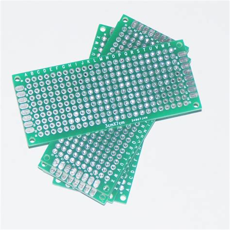
What is a PCB Prototype?
A PCB prototype, short for Printed Circuit Board prototype, is a preliminary version of a PCB design used for testing and validation before mass production. It allows engineers and designers to physically test the functionality, performance, and reliability of their PCB design in real-world conditions. PCB Prototyping is an essential step in the electronics manufacturing process, as it helps identify and rectify any design flaws or issues before committing to large-scale production.
Key Benefits of PCB Prototyping
- Design Validation: PCB Prototypes enable designers to test their designs in real-world conditions, ensuring the PCB functions as intended.
- Cost Savings: Identifying and fixing design issues during the prototyping stage can save significant costs compared to discovering problems during mass production.
- Improved Reliability: Thorough testing of PCB prototypes helps improve the overall reliability and durability of the final product.
- Faster Time-to-Market: PCB prototyping allows for parallel testing and validation, reducing the overall development time and enabling faster product launches.
Rayming’s PCB Prototype 3+3 Service
Rayming, a leading PCB manufacturer, offers a specialized PCB Prototype 3+3 Service to cater to the growing demand for rapid prototyping and short lead times. This service provides customers with three high-quality PCB prototypes within just three days, enabling faster design iterations and shorter time-to-market.
Key Features of Rayming’s PCB Prototype 3+3 Service
- Fast Turnaround: Rayming delivers three PCB prototypes within just three days, ensuring quick access to physical boards for testing and validation.
- High Quality: All PCB prototypes are manufactured using state-of-the-art equipment and undergo rigorous quality control processes to ensure the highest quality standards.
- Flexible Specifications: The 3+3 service supports a wide range of PCB specifications, including various materials, layer counts, and surface finishes.
- Cost-Effective: Rayming’s streamlined processes and optimized manufacturing techniques enable competitive pricing for PCB prototypes.
PCB Prototype Specifications Supported by Rayming’s 3+3 Service
| Specification | Options |
|---|---|
| PCB Material | FR-4, High Tg FR-4, Rogers, Aluminum, Flexible |
| Layer Count | 1-12 layers |
| Copper Thickness | 0.5 oz to 6 oz |
| PCB Thickness | 0.4 mm to 3.2 mm |
| Min. Hole Size | 0.2 mm |
| Min. Line Width | 0.1 mm |
| Solder Mask | Green, Red, Yellow, Blue, Black, White |
| Silkscreen | White, Black, Yellow |
| Surface Finish | HASL, ENIG, OSP, Immersion Silver, Immersion Gold |

Rayming’s PCB Prototype Manufacturing Process
Rayming follows a well-defined and optimized manufacturing process to ensure the timely delivery of high-quality PCB prototypes. The process involves the following steps:
- Design Review: Upon receiving the customer’s PCB design files, Rayming’s experienced engineers review the design for manufacturability and provide feedback if necessary.
- Material Selection: Based on the customer’s requirements and the PCB design, the appropriate materials are selected, including the PCB substrate, copper weight, and solder mask.
- PCB Fabrication: The PCB prototype is fabricated using advanced manufacturing techniques, including drilling, plating, etching, and lamination.
- Solder Mask Application: The selected solder mask color is applied to the PCB, protecting the copper traces and preventing short circuits.
- Silkscreen Printing: The chosen silkscreen color is printed onto the PCB, providing clear component labels and markings.
- Surface Finishing: The specified surface finish, such as HASL, ENIG, or OSP, is applied to the PCB to protect the exposed copper and enhance solderability.
- Electrical Testing: The PCB prototype undergoes rigorous electrical testing to ensure proper functionality and connectivity.
- Quality Control: Rayming’s quality control team inspects the PCB prototype for any defects or inconsistencies, ensuring compliance with the customer’s specifications.
- Packaging and Shipping: The PCB prototypes are carefully packaged and shipped to the customer within the promised three-day turnaround time.
Advantages of Choosing Rayming for PCB Prototype 3+3 Service
- Expertise: With years of experience in PCB manufacturing, Rayming has the knowledge and expertise to deliver high-quality PCB prototypes consistently.
- Advanced Equipment: Rayming invests in state-of-the-art manufacturing equipment and technology to ensure precise and reliable PCB prototyping.
- Quality Assurance: Stringent quality control measures are in place throughout the manufacturing process to guarantee the highest quality standards.
- Customer Support: Rayming’s dedicated customer support team is available to assist with any questions or concerns throughout the PCB prototyping process.
- Competitive Pricing: Despite the fast turnaround time and high quality, Rayming offers competitive pricing for its PCB Prototype 3+3 Service.

PCB Prototype Design Considerations
To ensure the best results when using Rayming’s PCB Prototype 3+3 Service, consider the following design guidelines:
- Adhere to the supported PCB specifications, including layer count, material, and thickness.
- Follow the recommended minimum hole size and line width to ensure manufacturability.
- Provide clear and accurate design files, preferably in Gerber or ODB++ Format.
- Specify the desired solder mask and silkscreen colors, as well as the surface finish.
- Allow for sufficient clearances between components and traces to avoid potential short circuits or manufacturing issues.
Common PCB Prototype Design Mistakes to Avoid
- Incorrect Footprint: Ensure that the component footprints in your PCB design match the actual components to be used.
- Insufficient Clearances: Maintain appropriate clearances between components, traces, and vias to prevent short circuits and manufacturing problems.
- Incorrect Drill Sizes: Specify the correct drill sizes for through-holes and vias to ensure proper plating and connectivity.
- Inconsistent Nets: Double-check that all nets in your PCB design are correctly connected and named.
- Incomplete Documentation: Provide comprehensive documentation, including assembly drawings and bill of materials (BOM), to avoid confusion during the manufacturing process.

Frequently Asked Questions (FAQ)
-
Q: What is the minimum order quantity for Rayming’s PCB Prototype 3+3 Service?
A: The minimum order quantity for Rayming’s PCB Prototype 3+3 Service is three pieces. -
Q: What file formats does Rayming accept for PCB prototype orders?
A: Rayming accepts PCB design files in Gerber or ODB++ format. -
Q: Can I request a different quantity of PCB prototypes other than three?
A: Yes, Rayming can accommodate different quantities of PCB prototypes. However, the 3+3 service specifically offers three pieces within a three-day turnaround time. -
Q: Does Rayming offer assembly services for PCB prototypes?
A: Yes, Rayming offers PCB Assembly services for prototypes. Please contact their customer support team for more information on assembly options. -
Q: What is the maximum layer count supported by Rayming’s PCB Prototype 3+3 Service?
A: Rayming’s PCB Prototype 3+3 Service supports up to 12 layers.
Conclusion
Rayming’s PCB Prototype 3+3 Service is an excellent choice for customers seeking fast, high-quality PCB prototypes. With a commitment to delivering three prototypes within three days, Rayming enables designers and engineers to accelerate their design validation and testing processes. By leveraging advanced manufacturing techniques, stringent quality control measures, and a wide range of supported PCB specifications, Rayming ensures that customers receive reliable and top-notch PCB prototypes. Whether you are developing a new product or iterating on an existing design, Rayming’s PCB Prototype 3+3 Service can help you achieve your goals faster and more efficiently.


Leave a Reply