What is PCB Panelization?
PCB panelization is the process of combining multiple printed Circuit board designs onto a single panel for manufacturing. This allows multiple PCBs to be fabricated at the same time, reducing costs and production time compared to manufacturing each PCB individually.
Panelization is especially beneficial for smaller PCBs and high volume production runs. Grouping multiple copies of a PCB design together onto larger panels makes the boards easier to handle during the fabrication process and assembly.
Why Panelize PCBs?
There are several key advantages to panelizing PCBs for production:
-
Lower costs – Fabricating multiple PCBs on a single panel reduces the cost per unit compared to making them individually. Setup and tooling costs are spread out over a larger number of boards.
-
Faster production – Panels allow a higher throughput in production since multiple boards can go through each process step together rather than one at a time. This shortens the overall production time.
-
Easier handling – Very small individual PCBs can be difficult to handle and transport between process steps. Combining them into panels makes them easier to work with.
-
Automated assembly – Many automated pick-and-place and soldering machines are designed to handle standard panel sizes. Panelization allows your PCBs to be compatible with these assembly lines.
Overall, panelization provides cost savings and efficiency improvements that are essential for commercial PCB Fabrication, especially for small boards and high volumes.
PCB Panelization Methods
There are two main approaches for panelizing PCBs:
Tab Routing Panelization
With tab routing, each individual PCB is connected to the main panel by small tabs. After fabrication, the individual boards can be separated from the main panel by snapping or cutting the tabs.
Some characteristics of tab routing include:
- Simple and inexpensive panelization method
- Leaves behind tab stubs on edges of individual PCBs
- Not suitable for boards with components or traces near edges
- Potential for rough or uneven edges after depaneling
V-Scoring Panelization
V-scoring uses a V-shaped groove cut partially through the panel between individual boards. This allows the boards to be easily snapped apart after assembly.
Some characteristics of V-scoring are:
- Cleaner edges after depaneling compared to tab routing
- Allows traces and components closer to board edges
- More expensive than tab routing
- Risk of stressing or damaging boards when depaneling
The best panelization method depends on the specific design of the PCBs and the production requirements. In general, V-scoring provides better results but tab routing may be adequate and more economical for simpler designs.

Designing Your Panels
Determine Panel Sizes
The first step is to determine what size panels you will be using. This depends on the capabilities of your PCB fabricator and assembler.
Common panel sizes include:
| Panel Size | Dimensions (mm) |
|---|---|
| 18″ x 24″ | 457 x 610 |
| 21″ x 24″ | 533 x 610 |
| 18″ x 21″ | 457 x 533 |
| 16″ x 18″ | 406 x 457 |
Consult with your manufacturing partners to determine what panel sizes they can accommodate. Also consider the dimensions of your individual PCB design to determine how many you can fit per panel.
Panelization Layout
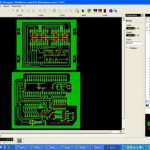
Next, create the layout of your PCBs on the panel. Determine the spacing between boards and the size of the tabs or V-score. Your manufacturer can provide guidance on their requirements and recommendations.
Some key considerations for panel layout:
- Provide enough space between PCBs for cutting/scoring plus manufacturing tolerances
- Ensure copper layers are not too close to board edges to avoid shorts
- Add tooling holes and fiducials to panels to assist fabrication and assembly
- Consider any text or labels you want on the panel
It’s a good idea to create your panel layouts using the same PCB design software you used for the individual boards. This ensures everything stays aligned and lets you verify the panel design against your board files.
V-Score Characteristics
If using V-scoring to panelize, there are a few specific parameters to consider:
| V-Score Parameter | Typical Value |
|---|---|
| V-Angle | 30° |
| Scoring Depth | 1/3 of board thickness |
| Spacing | > 3mm from components |
Confirm the exact specifications with your PCB fabricator as these may vary based on their capabilities and preferences. Getting the V-score design correct is critical to allowing clean, easy depaneling of the individual PCBs after assembly.
Preparing Files for Manufacturing
With your panelization layout complete, prepare the files to send to your manufacturer. This typically includes:
- Gerber files for each layer of the panel PCB
- NC drill files for any holes in the panel
- Fabrication drawings specifying panel dimensions, V-score parameters, etc.
- Pick & place and BOM files for assembly
Communicate clearly with your PCB manufacturer and assembler to ensure you are providing all the files they need in the correct formats. They can also do a design for manufacturing (DFM) check on your panel design to identify any potential issues before beginning production.
Depaneling
After your PCB panels have been fabricated and assembled, the final step is depaneling to separate the individual boards. The method depends on the type of panelization:
- Tab routed boards are typically depaneled using a shearing machine or by manually snapping the tabs.
- V-scored boards can be cleanly snapped apart by hand or with a simple tool.
Take care during depaneling to avoid damaging the individual PCBs. Rough handling can cause soldered components to come loose or place undue stress on the board.
After depaneling, inspect the individual boards to ensure there is no damage along the edges or to any components. The PCBs are now ready for final testing and integration into your end product.
FAQ
How many PCBs can I fit on a panel?
The number of PCBs per panel depends on two key factors:
- The dimensions of your individual PCB designs
- The size of the panels your manufacturer uses
Smaller PCBs allow more to be panelized together. Talk to your manufacturer about optimizing your panel layout to maximize the number of boards per panel and reduce costs.
What is the minimum spacing between boards on a panel?
For tab routing, the minimum space between PCBs is typically 2-3 mm to allow room for cutting the tabs. For V-scored panels, 3-5 mm is common to fit the scoring slots.
However, the exact spacing requirements depend on your manufacturer’s capabilities, so always verify their specifications before finalizing your panel design.
Can I panelize different PCB designs together?
Yes, you can often combine multiple different PCB designs onto a single panel, as long as they use the same materials and layer stackups. This is called an array panel.
Panelizing different designs together lets you optimize panel space usage and reduce costs when you need smaller quantities of each individual design. Your manufacturer can help advise the best way to lay out an array panel.
Do I need to panelize my PCBs?
Panelization is not always required but is recommended in most cases for commercial PCB fabrication. The main exception is for very large PCBs that already take up most of a panel size.
The cost and efficiency benefits of panelization make it worthwhile for the majority of small to medium sized PCB designs. Discuss with your manufacturer whether your specific design needs to be panelized.
Should I use tab routing or V-scoring?
The best method depends on your PCB design and production needs. Some general guidelines:
- Tab routing works well for simple 2-layer boards with larger components and traces kept away from the edges.
- V-scoring provides cleaner, more reliable results for denser boards or those that need traces/components near the edges.
The choice also comes down to your manufacturer’s capabilities and your budget. V-scoring is a more advanced technique and therefore costs more than tab routing in most cases.


Leave a Reply