Introduction to PCB Visualizer
In the world of electronics, Printed Circuit Boards (PCBs) play a crucial role in connecting and supporting various components to create functional devices. However, designing and analyzing these complex boards can be a daunting task, especially for beginners. This is where PCB Visualizer comes into the picture, offering a powerful and intuitive solution to streamline the PCB design process.
What is PCB Visualizer?
PCB Visualizer is a cutting-edge software tool that allows users to create, visualize, and analyze PCB designs in a user-friendly environment. It provides a comprehensive set of features and tools to simplify the PCB design workflow, making it accessible to both experienced professionals and hobbyists alike.
Key Features of PCB Visualizer
| Feature | Description |
|---|---|
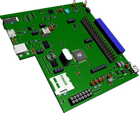
| 3D Visualization | Enables users to view their PCB designs in a realistic 3D environment, helping them identify potential issues and optimize the layout. |
| Real-time Collaboration | Allows multiple users to work on the same PCB design simultaneously, fostering teamwork and improving productivity. |
| Extensive Component Library | Provides a vast collection of pre-built components, making it easy to find and place the required elements on the PCB. |
| Intelligent Routing | Offers advanced algorithms to automate the routing process, ensuring optimal signal integrity and minimizing manual effort. |
| Design Rule Checking (DRC) | Performs automated checks to identify and resolve design issues, ensuring the PCB adheres to industry standards and manufacturing guidelines. |

Benefits of Using PCB Visualizer
1. Enhanced Design Efficiency
PCB Visualizer streamlines the design process by providing a user-friendly interface and powerful tools. With features like 3D visualization, real-time collaboration, and intelligent routing, designers can create complex PCB layouts quickly and efficiently.
2. Improved Collaboration and Communication
The real-time collaboration feature in PCB Visualizer enables team members to work together seamlessly, regardless of their physical location. This enhances communication, speeds up the design process, and ensures everyone is on the same page.
3. Reduced Errors and Rework
PCB Visualizer’s Design Rule Checking (DRC) functionality helps identify and resolve design issues early in the process. By catching errors before the PCB goes into production, designers can avoid costly rework and delays.
4. Increased Productivity and Time Savings
With an extensive component library and intelligent routing capabilities, PCB Visualizer significantly reduces the time and effort required to create PCB designs. Designers can focus on the critical aspects of the design, rather than spending hours on manual routing and component placement.

Getting Started with PCB Visualizer
System Requirements
To run PCB Visualizer smoothly, your system should meet the following minimum requirements:
- Operating System: Windows 10, macOS 10.15, or Linux (Ubuntu 18.04 or later)
- Processor: Intel Core i5 or equivalent
- RAM: 8 GB
- Graphics Card: Dedicated GPU with at least 2 GB VRAM
- Storage: 500 GB HDD or 256 GB SSD
Installation Process
Installing PCB Visualizer is a straightforward process. Follow these steps to get started:
- Visit the official PCB Visualizer website and download the installer for your operating system.
- Run the installer and follow the on-screen instructions to complete the installation.
- Launch PCB Visualizer and activate your license key.
- You’re now ready to start designing your PCBs!
Navigating the User Interface
PCB Visualizer offers an intuitive and user-friendly interface. Here’s an overview of the main sections:
| Section | Description |
|---|---|
| Toolbar | Contains various tools and options for designing and manipulating PCB elements. |
| Workspace | The main area where you create and edit your PCB designs. |
| Layers Panel | Allows you to manage and toggle the visibility of different layers in your PCB design. |
| Properties Panel | Displays and allows you to modify the properties of selected objects. |
| Library Panel | Provides access to the extensive component library for easy component placement. |

Design Workflow in PCB Visualizer
Step 1: Creating a New Project
To start a new PCB design, click on the “New Project” button in the toolbar or select “File” > “New Project” from the menu. Choose a project template or start from scratch, and specify the board dimensions and layer stackup.
Step 2: Placing Components
Drag and drop components from the Library Panel onto the workspace. You can search for specific components or browse through categories. Adjust the placement and orientation of the components as needed.
Step 3: Routing Connections
Use the routing tools in the toolbar to connect the components. PCB Visualizer offers both manual and automated routing options. The intelligent routing algorithms help optimize signal paths and minimize crosstalk.
Step 4: Design Rule Checking (DRC)
Regularly run DRC to identify and resolve any design issues. PCB Visualizer checks for common problems such as clearance violations, unconnected traces, and manufacturing constraints. Address the reported issues to ensure your design is error-free.
Step 5: 3D Visualization and Analysis
Switch to the 3D view to visualize your PCB design in a realistic environment. Rotate, pan, and zoom to examine the board from different angles. Use the analysis tools to assess signal integrity, thermal performance, and electromagnetic compatibility.
Step 6: Generating Manufacturing Files
Once your design is complete and passes DRC, generate the necessary manufacturing files. PCB Visualizer supports various output formats, including Gerber, Drill, and Pick and Place files. These files can be sent directly to PCB Manufacturers for production.
Advanced Features and Techniques
Scripting and Automation
PCB Visualizer supports scripting and automation through its built-in scripting language. Users can write custom scripts to automate repetitive tasks, create custom design rules, and extend the functionality of the software.
Multi-Board Design
For complex projects involving multiple interconnected PCBs, PCB Visualizer offers multi-board design capabilities. Designers can create and manage multiple PCBs within a single project, ensuring proper connectivity and synchronization between the boards.
Simulation and Analysis
PCB Visualizer integrates with various simulation and analysis tools to assess the performance and reliability of PCB designs. Users can perform signal integrity analysis, thermal simulation, and electromagnetic compatibility (EMC) analysis to optimize their designs and mitigate potential issues.
PCB Visualizer Community and Resources
PCB Visualizer Forums
The PCB Visualizer community is active and supportive, with dedicated forums where users can ask questions, share knowledge, and collaborate on projects. The forums are a great resource for troubleshooting, learning new techniques, and staying up to date with the latest developments in PCB design.
Online Tutorials and Courses
To help users get started and enhance their skills, PCB Visualizer offers a range of online tutorials and courses. These resources cover various topics, from basic PCB design concepts to advanced techniques and best practices. Users can learn at their own pace and access the materials anytime, anywhere.
User Documentation and Help Center
PCB Visualizer provides comprehensive user documentation and a dedicated Help Center. The documentation covers all aspects of the software, including installation, user interface, design workflow, and advanced features. The Help Center offers quick access to frequently asked questions, Troubleshooting Guides, and support resources.
Frequently Asked Questions (FAQ)
1. Is PCB Visualizer suitable for beginners?
Yes, PCB Visualizer is designed to be user-friendly and accessible to beginners. The intuitive interface, extensive component library, and automated features make it easy for even those with limited PCB design experience to get started.
2. Can PCB Visualizer handle complex PCB designs?
Absolutely. PCB Visualizer is equipped with powerful tools and advanced features to tackle complex PCB designs. It supports Multi-layer Boards, high-speed design, and advanced routing techniques to meet the demands of sophisticated projects.
3. Is PCB Visualizer compatible with other PCB design software?
PCB Visualizer supports industry-standard file formats, allowing seamless integration with other PCB design software. You can import and export designs in formats such as Gerber, ODB++, and IPC-2581, ensuring compatibility with a wide range of tools and manufacturers.
4. Does PCB Visualizer offer any collaboration features?
Yes, PCB Visualizer includes real-time collaboration features that enable multiple users to work on the same PCB design simultaneously. Team members can collaborate, share ideas, and make changes in real-time, regardless of their physical location.
5. How often is PCB Visualizer updated?
PCB Visualizer is actively developed and regularly updated to introduce new features, improvements, and bug fixes. The development team actively listens to user feedback and incorporates suggestions to enhance the software. Users can expect frequent updates and a continuously evolving feature set.
Conclusion
PCB Visualizer is a game-changer in the world of PCB design, offering a powerful and user-friendly solution for creating, visualizing, and analyzing PCBs. With its extensive features, intuitive interface, and active community, PCB Visualizer empowers designers of all skill levels to bring their electronic projects to life.
Whether you’re a seasoned professional or a hobbyist, PCB Visualizer provides the tools and resources you need to streamline your design process, collaborate effectively, and create high-quality PCBs. By embracing PCB Visualizer, you can unlock new possibilities in PCB design and take your projects to the next level.
So why wait? Start exploring the world of PCB Visualizer today and experience the future of PCB design!


Leave a Reply