Introduction to Soldermask and Nickel-Gold Surface Finish
Soldermask, also known as solder resist or solder mask, is a thin layer of polymer applied to the copper traces of a printed circuit board (PCB) to protect them from oxidation and prevent solder bridges during the soldering process. It also provides electrical insulation and helps to define the areas where solder should be applied. In the case of via-holes, soldermask plays a crucial role in ensuring the reliability and functionality of the PCB.
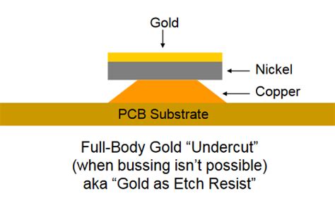
Nickel-gold (ENIG) is a popular surface finish for PCBs due to its excellent solderability, corrosion resistance, and durability. The chemical process involves plating a thin layer of nickel followed by a thin layer of gold on the exposed copper surfaces of the PCB. This surface finish is particularly suitable for high-reliability applications and fine-pitch components.
The Importance of Soldermask on Via-Holes
Via-holes are small holes drilled through the PCB to connect different layers of the board electrically. They are essential for creating multi-layer PCBs and ensuring proper signal routing. However, via-holes can also pose challenges during the manufacturing process and affect the overall reliability of the PCB.
Protection from Contamination
One of the primary functions of soldermask on via-holes is to protect them from contamination during the various stages of PCB manufacturing. Contaminants such as dust, debris, and chemical residues can accumulate inside the via-holes, leading to poor electrical connections and potential failures. By applying soldermask over the via-holes, the risk of contamination is significantly reduced.
Prevention of Solder Wicking
Solder wicking, also known as capillary action, is a phenomenon where molten solder is drawn into the via-holes during the soldering process. This can result in insufficient solder on the component pads, leading to weak solder joints and potential reliability issues. Soldermask on via-holes helps to prevent solder wicking by sealing the holes and restricting the flow of molten solder.
Electrical Insulation
Soldermask provides electrical insulation between the different layers of the PCB. When applied to via-holes, it prevents short circuits and ensures proper signal integrity. This is particularly important in high-density PCBs where the spacing between the via-holes is minimal.

Challenges in Applying Soldermask on Via-Holes
While soldermask on via-holes offers numerous benefits, there are also challenges associated with its application, especially in the case of chemical nickel-gold surface finish.
Compatibility with Nickel-Gold Surface Finish
One of the main challenges is ensuring compatibility between the soldermask and the nickel-gold surface finish. The chemical processes involved in applying the nickel-gold finish can affect the adhesion and integrity of the soldermask. It is essential to select a soldermask that is specifically formulated for use with nickel-gold surface finish to avoid any compatibility issues.
Uniform Coverage
Achieving uniform coverage of soldermask on via-holes can be challenging, particularly in high-density PCBs with small via-holes. Incomplete or uneven coverage can lead to exposed copper surfaces, which are susceptible to oxidation and contamination. This can result in poor electrical connections and reduced reliability.
Thickness Control
Controlling the thickness of the soldermask on via-holes is crucial for ensuring proper functionality and reliability. If the soldermask is too thin, it may not provide adequate protection and insulation. On the other hand, if it is too thick, it can interfere with the soldering process and lead to poor solder joint formation.

Best Practices for Applying Soldermask on Via-Holes
To overcome the challenges and ensure the successful application of soldermask on via-holes in the case of chemical nickel-gold surface finish, the following best practices should be followed:
-
Selection of Compatible Soldermask: Choose a soldermask that is specifically formulated for use with nickel-gold surface finish. This ensures optimal adhesion and compatibility between the soldermask and the surface finish.
-
Proper Surface Preparation: Before applying the soldermask, ensure that the PCB surface is clean, dry, and free from any contaminants. This can be achieved through proper cleaning and drying processes.
-
Optimized Application Process: Use an optimized application process that ensures uniform coverage of the soldermask on the via-holes. This may involve adjusting the soldermask viscosity, application pressure, and speed to achieve the desired results.
-
Thickness Control: Implement strict thickness control measures to ensure that the soldermask on via-holes is within the specified range. This can be achieved through regular monitoring and calibration of the application equipment.
-
Post-Application Inspection: Conduct thorough post-application inspections to verify the quality and integrity of the soldermask on via-holes. This may involve visual inspections, electrical testing, and cross-sectional analysis.

Advantages of Soldermask on Via-Holes with Nickel-Gold Surface Finish
When applied correctly, soldermask on via-holes in combination with chemical nickel-gold surface finish offers several advantages:
-
Enhanced Reliability: The combination of soldermask protection and the corrosion resistance of nickel-gold surface finish significantly enhances the reliability of the PCB. It prevents contamination, solder wicking, and oxidation, leading to improved long-term performance.
-
Improved Signal Integrity: Soldermask on via-holes provides excellent electrical insulation, reducing the risk of short circuits and ensuring proper signal integrity. This is particularly beneficial in high-frequency and high-speed applications.
-
Better Solderability: Nickel-gold surface finish offers excellent solderability, allowing for the formation of strong and reliable solder joints. The soldermask on via-holes ensures that the solder is confined to the desired areas, resulting in a more controlled and efficient soldering process.
-
Cost-Effectiveness: Although the application of soldermask on via-holes with nickel-gold surface finish may require additional processing steps, it can be a cost-effective solution in the long run. The enhanced reliability and performance of the PCB can reduce the need for rework and repairs, ultimately saving time and money.
Case Studies and Real-World Applications
To further illustrate the importance and benefits of soldermask on via-holes in the case of chemical nickel-gold surface finish, let’s look at some real-world applications and case studies.
Aerospace Industry
In the aerospace industry, PCBs are subjected to harsh environments and extreme conditions. The use of soldermask on via-holes with nickel-gold surface finish is common in this industry to ensure the highest level of reliability and performance. For example, in avionics systems, where PCBs are exposed to vibration, temperature fluctuations, and moisture, the combination of soldermask protection and nickel-gold surface finish helps to prevent failures and ensure long-term stability.
Medical Devices
Medical devices require PCBs with exceptional reliability and durability. Soldermask on via-holes with nickel-gold surface finish is often used in medical applications to ensure proper functionality and patient safety. For instance, in implantable medical devices, such as pacemakers, the soldermask on via-holes helps to prevent contamination and ensures electrical insulation, while the nickel-gold surface finish provides excellent biocompatibility and corrosion resistance.
Automotive Electronics
In the automotive industry, PCBs are exposed to harsh environmental conditions, such as extreme temperatures, vibrations, and moisture. Soldermask on via-holes with nickel-gold surface finish is widely used in automotive electronics to ensure reliable performance and long-term durability. For example, in engine control units (ECUs), the soldermask on via-holes helps to prevent short circuits and ensures proper signal integrity, while the nickel-gold surface finish offers excellent corrosion resistance and solderability.
Frequently Asked Questions (FAQ)
-
What is the purpose of soldermask on via-holes?
The purpose of soldermask on via-holes is to protect them from contamination, prevent solder wicking, and provide electrical insulation between the different layers of the PCB. -
Why is nickel-gold surface finish commonly used in combination with soldermask on via-holes?
Nickel-gold surface finish is commonly used in combination with soldermask on via-holes due to its excellent solderability, corrosion resistance, and compatibility with the soldermask material. -
What are the challenges in applying soldermask on via-holes with nickel-gold surface finish?
The main challenges include ensuring compatibility between the soldermask and the nickel-gold surface finish, achieving uniform coverage of the soldermask on the via-holes, and controlling the thickness of the soldermask. -
How can the challenges in applying soldermask on via-holes be overcome?
The challenges can be overcome by selecting a compatible soldermask, ensuring proper surface preparation, optimizing the application process, implementing strict thickness control measures, and conducting thorough post-application inspections. -
What are the advantages of using soldermask on via-holes with nickel-gold surface finish?
The advantages include enhanced reliability, improved signal integrity, better solderability, and cost-effectiveness in the long run.
Conclusion
Soldermask on via-holes in the case of chemical nickel-gold surface finish plays a crucial role in ensuring the reliability, functionality, and performance of PCBs. It provides protection from contamination, prevents solder wicking, and offers electrical insulation. While there are challenges associated with its application, following best practices and selecting compatible materials can help overcome these challenges.
The combination of soldermask on via-holes and nickel-gold surface finish offers numerous advantages, including enhanced reliability, improved signal integrity, better solderability, and cost-effectiveness. Real-world applications in industries such as aerospace, medical devices, and automotive electronics demonstrate the importance and benefits of this approach.
As PCB technology continues to advance and the demand for high-reliability electronics grows, the use of soldermask on via-holes with nickel-gold surface finish is expected to remain a popular choice among PCB Manufacturers and designers. By understanding the principles, challenges, and best practices associated with this approach, the industry can continue to produce PCBs that meet the highest standards of quality and performance.
| Parameter | Specification |
|---|---|
| Soldermask Material | Compatible with ENIG |
| Soldermask Thickness | 0.8-1.2 mils (20-30 µm) |
| Via-Hole Size | 0.2-0.5 mm |
| Nickel Plating Thickness | 3-6 µin (0.08-0.15 µm) |
| Gold Plating Thickness | 1-3 µin (0.03-0.08 µm) |
| Soldermask Coverage | 100% on via-holes |
| Solderability Test | ANSI/J-STD-003 |
| Insulation Resistance | >10^10 ohms |
| Temperature Cycling Test | -55°C to +125°C |
| Moisture Resistance Test | MIL-STD-202, Method 103 |


Leave a Reply