What is the Composition of the Outer PCB Layer?
The outer layer of a PCB is typically made of a thin, protective coating called solder mask or solder resist. This coating is usually composed of a polymer-based ink that is applied to the surface of the PCB through a screen-printing or photo-imaging process. The most common types of solder mask materials include:
- Liquid Photoimageable Solder Mask (LPSM)
- LPSM is a photopolymer-based ink that is applied as a liquid and then exposed to UV light to cure and harden.
-
It offers excellent resolution, adhesion, and resistance to solvents and high temperatures.
-
Dry Film Photoimageable Solder Mask (DFSM)
- DFSM is a solid photopolymer film that is laminated onto the PCB surface and then exposed to UV light to cure and harden.
-
It provides good coverage and uniformity but may have lower resolution compared to LPSM.
-
Liquid Screen-Printable Solder Mask (LSPSM)
- LSPSM is a non-photoimageable ink that is applied through a screen-printing process.
- It is less expensive and easier to apply than photoimageable solder masks but may have lower resolution and durability.
| Solder Mask Type | Composition | Application Method | Advantages | Disadvantages |
|---|---|---|---|---|
| LPSM | Photopolymer-based ink | Liquid application, UV curing | High resolution, excellent adhesion and resistance | Higher cost, more complex process |
| DFSM | Solid photopolymer film | Lamination, UV curing | Good coverage and uniformity | Lower resolution than LPSM |
| LSPSM | Non-photoimageable ink | Screen-printing | Lower cost, easier application | Lower resolution and durability |
What are the Functions of the Outer PCB Layer?
The outer layer of a PCB serves several critical functions that ensure the reliability and performance of the board:
Protection from Environmental Factors
The solder mask layer acts as a barrier that protects the underlying copper traces, pads, and vias from exposure to environmental factors such as:
– Oxidation: The outer layer prevents the copper from reacting with oxygen in the air, which can cause the formation of an insulating oxide layer that hinders electrical conductivity.
– Corrosion: The solder mask layer shields the copper from corrosive agents like moisture, chemicals, and pollutants that can degrade the metal over time.
– Physical damage: The outer layer provides a degree of mechanical protection against scratches, abrasions, and impacts that could otherwise damage the delicate copper features.
Insulation and Prevention of Short-Circuits
The solder mask layer serves as an insulating barrier between adjacent copper traces and pads, preventing accidental short-circuits that could occur if exposed copper areas come into contact with each other or with conductive materials. This insulation is particularly important in high-density PCB designs where the spacing between copper features is minimal.
Solder Control and Improved Solderability
The outer layer also plays a role in controlling the flow of solder during the assembly process. By selectively exposing certain areas of the copper (such as pads and vias) while covering others, the solder mask layer helps to:
– Prevent solder bridges: The solder mask ensures that solder only adheres to the exposed copper areas, reducing the risk of Solder Bridging between adjacent pads or traces.
– Improve solder joint reliability: The solder mask layer defines the boundaries of the solder joint, promoting the formation of a well-shaped and reliable connection between the component lead and the PCB pad.
– Enhance solder wettability: The exposed copper areas on the outer layer are often treated with a surface finish (such as HASL, ENIG, or OSP) that improves the wettability and solderability of the pads.
Aesthetic Enhancement and Labeling
In addition to its technical functions, the outer layer of a PCB also serves an aesthetic and informative purpose:
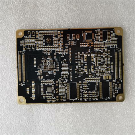
– Color coding: The solder mask layer can be pigmented in various colors (green, blue, red, black, etc.) to enhance the visual appearance of the PCB and make it easier to identify different board regions or components.
– Silkscreen printing: The outer layer can be printed with text, logos, and other markings using a silkscreen process, providing useful information such as component designators, polarity indicators, and assembly instructions.
How is the Outer PCB Layer Manufactured?
The manufacturing process for the outer layer of a PCB typically involves the following steps:
-
Copper etching: The bare PCB substrate is first etched to remove the unwanted copper, leaving only the desired traces, pads, and vias.
-
Surface cleaning: The etched PCB is cleaned to remove any residues or contaminants that could affect the adhesion of the solder mask.
-
Solder mask application: The solder mask material is applied to the PCB surface using one of the methods described earlier (LPSM, DFSM, or LSPSM).
-
Exposure and development (for photoimageable solder masks):
- The solder mask-coated PCB is exposed to UV light through a photomask that defines the areas where the solder mask should be removed.
-
The unexposed areas of the solder mask are then chemically developed and removed, exposing the underlying copper.
-
Curing: The solder mask is cured using heat or UV light to fully polymerize and harden the material.
-
Surface finish application: A surface finish (such as HASL, ENIG, or OSP) is applied to the exposed copper areas to improve solderability and protect against oxidation.
-
Silkscreen printing: If required, the outer layer is printed with text, logos, or other markings using a silkscreen process.
-
Final inspection: The completed PCB is inspected for any defects or irregularities in the outer layer, such as pinholes, cracks, or misaligned features.

FAQ
1. What is the difference between solder mask and solder resist?
Solder mask and solder resist are two terms that refer to the same thing – the protective coating applied to the outer layer of a PCB. The terms are often used interchangeably in the industry.
2. Can the outer layer of a PCB be repaired if damaged?
In some cases, minor damage to the outer layer (such as small scratches or pinholes) can be repaired using specialized solder mask repair kits or by applying a patch of solder mask material. However, extensive damage may require the PCB to be replaced entirely.
3. What is the typical thickness of the outer layer on a PCB?
The thickness of the solder mask layer can vary depending on the specific material and application method used, but it typically ranges from 0.0005 to 0.002 inches (0.0127 to 0.0508 mm).
4. Can the color of the outer layer affect the performance of the PCB?
The color of the solder mask layer is primarily for aesthetic purposes and does not directly impact the electrical performance of the PCB. However, some colors may be more or less susceptible to UV degradation over time, which could affect the long-term durability of the outer layer.
5. Are there any environmental concerns associated with the materials used in the outer layer of a PCB?
Some older solder mask formulations contained hazardous substances such as lead or volatile organic compounds (VOCs). However, modern solder mask materials are generally designed to be RoHS (Restriction of Hazardous Substances) compliant and have minimal environmental impact when properly handled and disposed of.
In conclusion, the outer layer of a PCB, composed of solder mask or solder resist, is a critical component that serves to protect the board from environmental factors, prevent short-circuits, improve solderability, and enhance aesthetics. By understanding the composition, functions, and manufacturing process of the outer PCB layer, designers and manufacturers can ensure the production of high-quality, reliable PCBs for a wide range of applications.
Leave a Reply