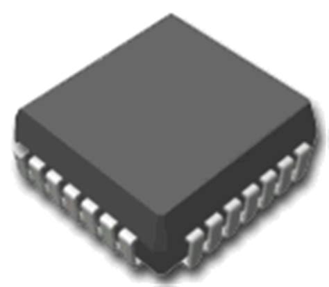
What is a PLCC Package?
PLCC stands for Plastic Leaded Chip Carrier. It is a surface-mount integrated circuit package used for housing and protecting electronic chips and providing electrical connections between the chip and a printed circuit board (PCB). PLCC Packages are square or rectangular in shape and have pins (leads) extending from all four sides, typically in a J-lead configuration where the pins are bent downward in a J shape.
Key characteristics of PLCC packages include:
- Plastic molded body
- J-shaped leads on all four sides
- Square or rectangular shape
- Low profile compared to through-hole packages
- Surface mount design for PCB Assembly
- Commonly used for microcontrollers, memories, ASICs, and other ICs
PLCC packages provide a compact, reliable, and cost-effective solution for many electronic applications. They allow high-density PCB designs and are compatible with automated assembly processes like pick-and-place machines and reflow soldering.
Advantages of PLCC Packages
PLCC packages offer several advantages over other IC packaging options:
1. Compact Size
The square/rectangular shape and J-lead design of PLCCs enable a smaller footprint compared to through-hole DIP packages. This allows higher component density on PCBs.
2. Low Profile
PLCCs have a lower profile than through-hole packages, which is beneficial for slim product designs and applications with limited vertical space.
3. Good Thermal Performance
The exposed pad on the bottom of many PLCC packages provides an efficient thermal path to dissipate heat from the chip to the PCB. This improves the thermal performance and reliability of the device.
4. Compatibility with Surface Mount Assembly
PLCC packages are designed for surface mount technology (SMT) assembly. They are compatible with pick-and-place machines and can be soldered using reflow methods. SMT Assembly enables high-volume, automated production.
5. Mechanical Stability
The J-leads on all four sides of a PLCC package provide good mechanical stability and strong solder joints. This enhances the reliability and durability of the assembLED PCB.
6. Moderate Lead Count
PLCCs typically have a moderate number of leads (e.g., 20 to 84), which is sufficient for many types of ICs. The lead count is higher than small outline packages but lower than fine-pitch BGA packages.
7. Socketed or Soldered Mounting
PLCCs can be directly soldered to the PCB for a permanent connection, or they can be inserted into a PLCC socket for easy removal and replacement. Socketed mounting is useful for prototyping, testing, and field upgrades.

PLCC Package Variations
There are several variations of PLCC packages to accommodate different chip sizes, lead counts, and application requirements:
| Package | Description | Lead Count Range | Body Size (mm) |
|---|---|---|---|
| PLCC | Standard PLCC with J-leads on all four sides | 20 to 84 | 8.5 to 30.6 |
| PQFP | Plastic Quad Flat Pack, similar to PLCC but with gull-wing leads | 32 to 256 | 7 to 28 |
| SOJ | Small Outline J-leaded, smaller than PLCC | 20 to 56 | 5.3 to 15.9 |
| QFJ | Quad Flat J-leaded, larger than PLCC | 100 to 256 | 14 to 40 |
These variations offer different trade-offs in terms of size, lead count, and manufacturability to suit specific design requirements.

How to Use PLCC Packages
Using PLCC packages involves several steps in the PCB design and assembly process:
1. PCB Footprint Design
Create the appropriate footprint for the PLCC package on the PCB layout. The footprint should match the package dimensions, lead pitch, and pad size. Consult the package datasheet or use standard footprint libraries in your PCB design software.
2. Schematic Design
In the schematic, represent the PLCC component with the correct symbol and pin assignments. Ensure that the symbol matches the actual package pinout.
3. PCB Layout
Place the PLCC footprint on the PCB and route the traces to connect the package pads to other components and power/ground planes. Follow good layout practices, such as providing proper power and ground connections, minimizing trace lengths, and avoiding signal integrity issues.
4. Solder Paste Stencil
For reflow soldering, use a solder paste stencil to apply solder paste to the PLCC pads on the PCB. The stencil apertures should match the pad size and shape.
5. Pick and Place
Use a pick-and-place machine to automatically place the PLCC package onto the PCB. The machine picks up the package from a tape or tray and aligns it with the footprint on the board.
6. Reflow Soldering
Pass the PCB through a reflow oven to melt the solder paste and form a permanent solder joint between the PLCC leads and the PCB pads. Follow the recommended reflow temperature profile for the specific solder paste and package.
7. Inspection and Testing
After soldering, visually inspect the solder joints for any defects or irregularities. Use automated optical inspection (AOI) or X-ray inspection for more thorough analysis. Perform functional testing to verify that the assembled PCB operates as intended.

PLCC Socket Mounting
In some cases, PLCC packages are mounted using sockets instead of direct soldering. PLCC sockets provide a removable and replaceable connection between the package and the PCB. They are commonly used for prototyping, testing, or field upgrades where easy component swapping is desirable.
To use a PLCC socket:
- Choose a socket compatible with the specific PLCC package (e.g., pin count, pitch).
- Solder the socket to the PCB using through-hole or surface mount techniques.
- Align the PLCC package with the socket and gently press it into place. The J-leads of the package should snap into the socket contacts.
- To remove the PLCC package from the socket, use a PLCC extraction tool or gently pry it out with a flathead screwdriver.
PLCC sockets offer flexibility and convenience but may introduce additional contact resistance and mechanical stress compared to direct soldering.
FAQ
1. What is the difference between PLCC and QFP packages?
PLCC (Plastic Leaded Chip Carrier) and QFP (Quad Flat Package) are both surface mount packages, but they have some differences:
- Lead Style: PLCC has J-leads bent downward, while QFP has gull-wing leads extending outward.
- Footprint: PLCC has a square footprint, while QFP is rectangular.
- Lead Count: PLCC typically has a lower lead count (up to 84) compared to QFP (up to 256).
- Socketing: PLCC packages can be socketed, while QFP packages are generally soldered directly.
2. Can PLCC packages be used for high-frequency applications?
PLCC packages can be used for high-frequency applications, but they may have some limitations compared to packages specifically designed for high-speed signaling (e.g., BGA, QFN). The J-leads of PLCC packages introduce parasitic inductance and capacitance, which can affect signal integrity at high frequencies. Proper PCB layout techniques and signal conditioning can help mitigate these effects.
3. Are PLCC packages suitable for high-power devices?
PLCC packages can be used for moderate-power devices, but they may not be the best choice for high-power applications. The exposed pad on the bottom of some PLCC packages helps with heat dissipation, but the thermal performance is limited by the package size and lead configuration. For high-power devices, packages with better thermal characteristics (e.g., QFN, TO-220) or additional heatsinking may be necessary.
4. How do I choose the right PLCC package for my application?
When selecting a PLCC package, consider the following factors:
- Chip size and lead count: Ensure the package can accommodate the chip and has enough leads for all the necessary connections.
- Thermal requirements: Consider the power dissipation of the device and choose a package with adequate thermal performance.
- PCB layout and assembly: Evaluate the PCB space constraints, routing complexity, and assembly process compatibility.
- Cost and availability: Consider the cost of the package and its availability from suppliers.
Consult the device datasheet, application notes, and package selection guides from manufacturers to make an informed decision.
5. Can PLCC packages be used in harsh environments?
PLCC packages can be used in harsh environments, but they may require additional protection or qualification. The plastic molding compound of PLCC packages provides some level of moisture and mechanical protection, but it is not hermetically sealed. For extreme environmental conditions (e.g., high humidity, corrosive gases, extreme temperatures), specialized packaging options (e.g., ceramic, metal-can) or conformal coating may be necessary. Always consider the specific environmental requirements and consult the device manufacturer for guidance.
Conclusion
PLCC (Plastic Leaded Chip Carrier) packages are widely used in the electronics industry for housing and connecting various types of integrated circuits. They offer a compact, low-profile, and surface-mountable solution with good mechanical stability and moderate lead count. PLCC packages are available in different variations to suit specific application needs and can be soldered directly to the PCB or used with sockets for easy replacement.
When using PLCC packages, proper PCB footprint design, schematic representation, and layout techniques are crucial for ensuring reliable and efficient assembly. The package selection process should consider factors such as chip size, thermal requirements, PCB layout, cost, and environmental conditions.
While PLCC packages have some limitations in terms of high-frequency performance and power dissipation compared to more advanced package types, they remain a popular choice for many electronic applications due to their versatility, reliability, and cost-effectiveness.
As with any electronic packaging technology, staying informed about industry trends, new package variations, and best practices is essential for making informed design decisions and achieving successful product development.


Leave a Reply