Introduction to Monostable Designs
A monostable multivibrator, also known as a oneshot or a single-shot circuit, is a popular and versatile electronic circuit that generates a single output pulse in response to an input trigger signal. The 555 timer IC is commonly used to create monostable designs due to its simplicity, reliability, and wide range of applications. In this article, we will explore the fundamentals of monostable designs, focusing on the 555 oneshot circuit and its various configurations.
What is a Monostable Multivibrator?
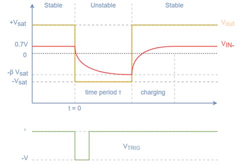
A monostable multivibrator is an electronic circuit that has two stable states: a stable state and a quasi-stable state. When the circuit is in its stable state, it remains in that state indefinitely until an external trigger signal is applied. Once triggered, the circuit transitions to its quasi-stable state, where it remains for a predetermined duration before automatically returning to its stable state.
The time spent in the quasi-stable state is determined by the values of the external components connected to the 555 timer IC, such as resistors and capacitors. This time duration is often referred to as the “pulse width” or “time constant” of the monostable circuit.
Applications of Monostable Designs
Monostable designs have a wide range of applications in electronics and control systems. Some common use cases include:
- Pulse generation: Monostable circuits can generate precise, fixed-duration pulses for triggering other circuits or systems.
- Debouncing switches: Mechanical switches often produce multiple, rapid transitions when pressed or released. A monostable circuit can be used to clean up these transitions and provide a single, clean output pulse.
- Timing control: Monostable designs can be used to introduce precise time delays or to control the duration of events in various systems.
- Alarm systems: Monostable circuits can be used to generate audible or visual alarms for a specific duration when triggered by an event.
- Pulse-Width Modulation (PWM): By varying the time constant of a monostable circuit, it is possible to generate PWM signals with adjustable duty cycles.
555 Timer IC Overview
The 555 timer IC is an incredibly versatile and widely used integrated circuit that can be configured to operate in various modes, including monostable, astable, and bistable. In this section, we will focus on the 555 timer’s internal structure and its operation in monostable mode.
555 Timer IC Pinout
The 555 timer IC is available in an 8-pin DIP (Dual Inline Package) or an 8-pin SOIC (Small Outline Integrated Circuit) package. The pinout for the 555 timer is as follows:
| Pin Number | Pin Name | Description |
|---|---|---|
| 1 | GND | Ground |
| 2 | TRIG | Trigger input (active low) |
| 3 | OUT | Output pin |
| 4 | RESET | Reset input (active low) |
| 5 | CTRL | Control voltage input |
| 6 | THR | Threshold input |
| 7 | DIS | Discharge pin (open-collector output) |
| 8 | VCC | Positive supply voltage (typically 5V to 15V) |
Internal Structure of the 555 Timer
The 555 timer IC consists of several key components that work together to achieve its functionality:
- Voltage divider: A three-resistor voltage divider network that provides reference voltages for the comparators. The reference voltages are set at 1/3 VCC and 2/3 VCC.
- Comparators: Two comparators that compare the voltage at the TRIG and THR pins with the reference voltages from the voltage divider. The output of the comparators controls the state of the flip-flop.
- Flip-flop: A bistable flip-flop that changes state based on the outputs of the comparators. The flip-flop’s output controls the output stage and the discharge transistor.
- Output stage: A push-pull output stage that provides a high or low output signal at the OUT pin, depending on the state of the flip-flop.
- Discharge transistor: An open-collector NPN transistor that is used to discharge the external timing capacitor when the flip-flop is in the reset state.
Basic 555 Monostable Circuit
A basic 555 monostable circuit can be constructed using a few external components connected to the 555 timer IC. In this section, we will discuss the circuit diagram, component selection, and operation of the basic 555 monostable circuit.
Circuit Diagram
The circuit diagram for a basic 555 monostable circuit is shown below:
           +5V to +15V
            |
            |
            |
           +-+
           |8|
           | |
      +----+7+----+
      |    | |    |
     +-+   | |   +-+
     |6|   |5|   |4|
     | |   | |   | |
     +-+   +-+   +-+
      |     |     |
      |     |     |
     +++   +++   +++
     | |   | |   | |
     | |   | |   | |
     | |   | |   | |
     +-+   +-+   +-+
     |3|   |2|   |1|
     | |   | |   | |
    OUT   TRIG  GND
Component Selection
To create a 555 monostable circuit, you will need the following components:
- 555 timer IC
- Resistor (R): The value of the resistor determines the duration of the output pulse. Typical values range from 1 kΩ to 1 MΩ.
- Capacitor (C): The value of the capacitor also affects the pulse duration. Typical values range from 0.1 µF to 1000 µF.
The pulse duration (T) of the monostable circuit can be calculated using the following formula:
T = 1.1 × R × C
Where:
– T is the pulse duration in seconds
– R is the resistance in ohms (Ω)
– C is the capacitance in farads (F)
Circuit Operation
The operation of the basic 555 monostable circuit can be summarized as follows:
- Initially, the capacitor C is discharged, and the TRIG pin is held high (above 1/3 VCC).
- When a negative-going trigger pulse is applied to the TRIG pin, the voltage at TRIG falls below 1/3 VCC, causing the output of the lower comparator to go high.
- The high output of the lower comparator sets the flip-flop, which drives the OUT pin high and turns off the discharge transistor.
- With the discharge transistor off, the capacitor C begins to charge through the resistor R towards VCC.
- When the voltage across the capacitor reaches 2/3 VCC, the upper comparator’s output goes high, resetting the flip-flop.
- The flip-flop’s reset causes the OUT pin to go low and turns on the discharge transistor, rapidly discharging the capacitor C.
- The circuit remains in this state until another trigger pulse is applied to the TRIG pin.

Advanced 555 Monostable Configurations
While the basic 555 monostable circuit is suitable for many applications, there are several advanced configurations that offer additional features and benefits. In this section, we will explore two popular advanced 555 monostable configurations: retriggerable monostable and cascaded monostable circuits.
Retriggerable Monostable Circuit
A retriggerable monostable circuit allows the output pulse duration to be extended by applying additional trigger pulses during the initial output pulse. This feature is useful in applications where the output pulse duration needs to be prolonged based on external events or conditions.
To create a retriggerable monostable circuit, a diode is added between the TRIG pin and the junction of the resistor and capacitor. The diode prevents the capacitor from discharging through the TRIG pin when subsequent trigger pulses are applied.
           +5V to +15V
            |
            |
            |
           +-+
           |8|
           | |
      +----+7+----+
      |    | |    |
     +-+   | |   +-+
     |6|   |5|   |4|
     | |   | |   | |
     +-+   +-+   +-+
      |     |     |
      |     |     |
     +++   +++   +++
     | |   | |   | |
     | |   | |   | |
     | |   | |   | |
     +-+   +-+   +-+
     |3|   |2|   |1|
     | |   | |   | |
    OUT   TRIG  GND
           |
           |
           -
         |<  |
           -
           |
           |
          +++
          | |
          | |
          | |
          +-+
In this configuration, each subsequent trigger pulse applied to the TRIG pin during the initial output pulse will recharge the capacitor and extend the output pulse duration.
Cascaded Monostable Circuits
Cascaded monostable circuits involve connecting two or more 555 monostable stages in series to create a sequence of output pulses with specific durations and delays. This configuration is useful in applications that require complex timing sequences or multiple, precisely timed events.
In a cascaded monostable circuit, the output of the first stage triggers the second stage, and so on. The duration of each stage’s output pulse is determined by its respective resistor and capacitor values.
 Stage 1         Stage 2
  +-----+        +-----+
  |     |        |     |
  |  555|        |  555|
  |     |        |     |
  +-----+        +-----+
   |  |           |  |
   |  +---R1---+  |  +---R2---+
   |           |  |           |
   +---C1------+  +---C2------+
      |               |
     GND             GND
By carefully selecting the resistor and capacitor values for each stage, you can create a wide variety of timing sequences and delay patterns.
Troubleshooting 555 Monostable Circuits
When working with 555 monostable circuits, you may encounter issues or unexpected behavior. In this section, we will discuss common problems and their solutions to help you troubleshoot your 555 monostable designs effectively.
Incorrect Pulse Duration
If the output pulse duration is not as expected, consider the following:
- Check the values of the resistor and capacitor: Ensure that the resistor and capacitor values are correct and match your desired pulse duration according to the formula T = 1.1 × R × C.
- Verify component tolerances: Resistors and capacitors have tolerances that can affect the pulse duration. Use components with tighter tolerances for more precise timing.
- Check for leakage: Ensure that the capacitor is not leaking, as this can cause the pulse duration to be shorter than expected. Use high-quality, low-leakage capacitors for best results.
Unstable or Oscillating Output
If the output is unstable or oscillating, consider the following:
- Decouple the power supply: Add a 0.1 µF ceramic capacitor between the VCC and GND pins of the 555 timer IC to minimize power supply noise and instability.
- Check for proper grounding: Ensure that all ground connections are properly made and that there are no ground loops or other grounding issues in your circuit.
- Use proper Bypass Capacitors: Place ceramic bypass capacitors (0.1 µF to 1 µF) close to the VCC and GND pins of the 555 timer IC to provide a low-impedance path for high-frequency noise.
Trigger Issues
If the circuit is not triggering correctly, consider the following:
- Check the trigger signal: Ensure that the trigger signal is a clean, negative-going pulse that crosses the 1/3 VCC threshold. Use an oscilloscope to verify the trigger signal’s characteristics.
- Verify the TRIG pin connection: Ensure that the TRIG pin is properly connected to the trigger source and that there are no shorts or open circuits.
- Check for proper pull-up: If the TRIG pin is left floating, it may cause erratic triggering. Connect a pull-up resistor (10 kΩ to 100 kΩ) between the TRIG pin and VCC to ensure a stable trigger input.
FAQ
-
Q: What is the main difference between a monostable and an astable multivibrator?
A: A monostable multivibrator generates a single output pulse of a fixed duration in response to a trigger signal, while an astable multivibrator continuously oscillates between two states, generating a square wave output. -
Q: Can a 555 monostable circuit be triggered by a positive-going pulse?
A: No, a standard 555 monostable circuit is triggered by a negative-going pulse that pulls the TRIG pin below 1/3 VCC. However, you can invert the trigger signal using an additional transistor or logic gate to achieve triggering on a positive-going pulse. -
Q: How do I calculate the resistor and capacitor values for a desired pulse duration?
A: To calculate the resistor and capacitor values, use the formula T = 1.1 × R × C, where T is the desired pulse duration in seconds, R is the resistance in ohms (Ω), and C is the capacitance in farads (F). Choose a suitable capacitor value and then calculate the required resistor value using the formula R = T / (1.1 × C). -
Q: Can I use a 555 monostable circuit to generate pulses longer than a few minutes?
A: While it is possible to generate long pulses with a 555 monostable circuit, it may not be practical due to the large resistor and capacitor values required. For pulses longer than a few minutes, consider using a microcontroller or a dedicated long-duration timer IC. -
Q: What is the maximum supply voltage for a 555 timer IC?
A: The maximum supply voltage for a standard 555 timer IC is typically 16V. However, some manufacturers offer low-voltage versions that can operate down to 2V and high-voltage versions that can handle up to 18V. Always consult the manufacturer’s datasheet for the specific voltage range of your 555 timer IC.
Conclusion
Monostable designs based on the 555 timer IC offer a simple, reliable, and versatile solution for generating single output pulses with precise durations. By understanding the internal structure of the 555 timer, the basic 555 monostable circuit, and advanced configurations like retriggerable and cascaded monostable circuits, you can create a wide range of timing and control applications.
When designing and troubleshooting 555 monostable circuits, pay close attention to component selection, proper grounding, and power supply decoupling to ensure stable and accurate operation. By following best practices and understanding common issues, you can effectively incorporate 555 monostable designs into your projects and take advantage of their flexibility and robustness.
As you explore the world of 555 monostable circuits, be sure to consult datasheets, application notes, and online resources for more in-depth information and creative design ideas. With its enduring popularity and extensive documentation, the 555 timer IC will continue to be a valuable tool in the electronics designer’s toolkit for years to come.


Leave a Reply