Introduction to Vias and Via Plugging
In the world of printed circuit board (PCB) design and manufacturing, vias play a crucial role in connecting different layers of a multi-layer PCB. Vias are essentially small holes drilled through the PCB that allow electrical connections to be made between different layers. While vias are essential for creating complex and compact PCB designs, they can also introduce challenges, particularly when it comes to the assembly process and ensuring the reliability of the final product.
One technique that is often employed to address these challenges is via plugging. Via plugging involves filling the vias with a non-conductive material, such as epoxy or a specialized via filling paste, to create a smooth, planar surface on the PCB. This process can offer several benefits, including improved reliability, better manufacturing yields, and enhanced aesthetics.
However, via plugging also comes with its own set of considerations and trade-offs. It can add complexity and cost to the manufacturing process, and in some cases, it may not be necessary or even desirable. In this article, we will delve into the topic of Plugged Vias, exploring the reasons why via plugging is used, the different methods and materials employed, and the factors to consider when deciding whether or not to plug your vias.
The Purpose of Via Plugging
Preventing Solder Wicking
One of the primary reasons for plugging vias is to prevent solder wicking during the assembly process. Solder wicking occurs when molten solder is drawn into the via hole through capillary action during the soldering process. This can lead to several problems, including:
- Insufficient solder on the component pad, resulting in a weak or unreliable solder joint
- Excess solder on the opposite side of the board, which can cause short circuits or interfere with other components
- Difficulty in inspecting and testing the solder joint, as the solder is hidden within the via
By plugging the vias, the solder is prevented from being drawn into the hole, ensuring a proper solder joint on the component pad and minimizing the risk of solder-related defects.
Improving Reliability
Via plugging can also help to improve the overall reliability of the PCB. In harsh environments, such as those with high humidity or frequent temperature cycling, unplugged vias can act as conduits for moisture and contaminants to enter the PCB. This can lead to corrosion, delamination, and other reliability issues over time.
By sealing the vias with a non-conductive material, the entry points for moisture and contaminants are eliminated, thus enhancing the long-term reliability of the PCB. This is particularly important for applications where reliability is critical, such as in aerospace, automotive, and medical devices.
Enhancing Manufacturing Yields
Via plugging can also help to improve manufacturing yields, particularly in high-volume production. Unplugged vias can cause several manufacturing-related issues, such as:
- Difficulty in applying solder paste or other adhesives, as the material can seep into the vias
- Uneven surface for component placement, leading to misaligned or poorly seated components
- Challenges in applying conformal coatings or other protective layers, as the vias can create voids or air pockets
By creating a smooth, planar surface through via plugging, these manufacturing challenges can be minimized, resulting in higher yields and fewer defects.
Improving Aesthetics
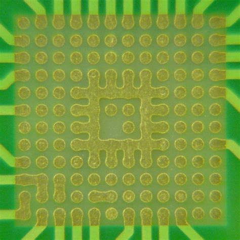
In some applications, the appearance of the PCB is important, such as in consumer electronics or high-end audio equipment. Unplugged vias can detract from the visual appeal of the PCB, creating a “swiss cheese” effect with numerous holes visible on the surface.
Via plugging can help to create a cleaner, more polished look by eliminating the visible holes and creating a smooth, uniform surface. This can be particularly important for PCBs that are visible to the end-user or that are used in products where aesthetics are a key selling point.
Methods and Materials for Via Plugging
There are several methods and materials that can be used for via plugging, each with its own advantages and disadvantages. The choice of method and material will depend on factors such as the size and depth of the vias, the desired performance characteristics, and the manufacturing process being used.
Epoxy Filling
One of the most common methods for via plugging is epoxy filling. This involves dispensing a liquid epoxy material into the vias, which then hardens to create a solid, non-conductive plug. Epoxy filling can be done manually, using a syringe or needle to dispense the material, or automatically, using specialized equipment that can fill multiple vias simultaneously.
Advantages of epoxy filling include:
- Good flow characteristics, allowing the epoxy to fill the vias completely without air pockets
- Strong adhesion to the via walls, creating a secure and reliable plug
- Wide availability of epoxy materials with different properties, such as thermal conductivity or flexibility
Disadvantages of epoxy filling include:
- Longer curing times compared to other methods, which can impact manufacturing throughput
- Potential for voids or air pockets if the epoxy is not dispensed properly
- Difficulty in removing the epoxy if rework or repair is needed
Via Filling Pastes
Another option for via plugging is the use of specialized via filling pastes. These pastes are typically based on a polymer resin filled with non-conductive particles, such as silica or ceramic. The paste is screen printed onto the PCB, filling the vias in the process. The paste is then cured using heat or UV light to create a solid, non-conductive plug.
Advantages of via filling pastes include:
- Fast curing times, allowing for high-throughput manufacturing
- Good planarization, creating a smooth surface for component placement
- Compatibility with standard PCB manufacturing processes, such as screen printing
Disadvantages of via filling pastes include:
- Limited flow characteristics compared to epoxy, which can result in incomplete filling of deep or narrow vias
- Higher material costs compared to epoxy
- Potential for shrinkage or cracking during curing, which can impact reliability
Conductive Via Filling
In some cases, it may be desirable to fill the vias with a conductive material, rather than a non-conductive one. This is known as conductive via filling, and it can be used to create low-resistance electrical connections between layers or to improve Thermal dissipation.
Conductive via filling materials include:
- Silver-filled epoxies
- Copper-filled pastes
- Solder pastes
Advantages of conductive via filling include:
- Improved electrical performance, with lower resistance and inductance
- Enhanced thermal conductivity, allowing for better heat dissipation
- Potential for increased reliability, as the conductive material can help to reinforce the via structure
Disadvantages of conductive via filling include:
- Higher material costs compared to non-conductive filling options
- Potential for shorts or unintended electrical connections if the filling process is not well-controlled
- Compatibility issues with certain surface finishes or soldering processes

Factors to Consider When Deciding to Plug Vias
When deciding whether or not to plug vias in a PCB design, there are several factors that should be considered. These include:
PCB Application and Environment
The intended application and operating environment of the PCB should be a key factor in the decision to plug vias. For example, PCBs that will be used in harsh environments, such as those with high humidity, extreme temperatures, or exposure to chemicals, may benefit from via plugging to improve reliability and prevent contamination.
On the other hand, PCBs used in less demanding environments or in applications where reliability is less critical may not require via plugging, as the added cost and complexity may not be justified.
Manufacturing Process and Capabilities
The manufacturing process and capabilities of the PCB fabricator should also be considered when deciding to plug vias. Some fabricators may have specialized equipment and expertise in via plugging, while others may not offer this service or may have limited capabilities.
It is important to discuss via plugging requirements with the fabricator early in the design process to ensure that they can accommodate the desired method and material. In some cases, the fabricator may recommend alternative methods or materials based on their experience and capabilities.
Cost and Time Considerations
Via plugging can add cost and time to the PCB manufacturing process, which should be factored into the decision-making process. The cost of via plugging will depend on the method and material used, as well as the number and size of the vias to be plugged.
In addition to material costs, via plugging can also add labor and equipment costs to the manufacturing process. This can impact the overall cost of the PCB, as well as the lead time for production.
It is important to weigh the potential benefits of via plugging, such as improved reliability or manufacturing yields, against the added cost and time required. In some cases, the benefits may outweigh the costs, while in others, the added expense may not be justified.
Design Considerations
The PCB design itself can also impact the decision to plug vias. Factors such as the number and density of vias, the layer stack-up, and the component placement can all affect the need for via plugging.
For example, PCBs with a high density of vias or with vias located close to component pads may be more susceptible to solder wicking and may benefit from via plugging. Similarly, PCBs with a large number of layers or with blind or buried vias may require via plugging to ensure reliable connections between layers.
Designers should consider these factors when deciding whether or not to plug vias, and should work closely with the fabricator to ensure that the design is compatible with the chosen via plugging method and material.
FAQ
-
What is via plugging, and why is it used?
Via plugging is the process of filling vias with a non-conductive material to create a smooth, planar surface on the PCB. It is used to prevent solder wicking, improve reliability, enhance manufacturing yields, and improve aesthetics. -
What materials are commonly used for via plugging?
Common materials for via plugging include epoxy, specialized via filling pastes, and conductive materials such as silver-filled epoxies or copper-filled pastes. -
What factors should be considered when deciding to plug vias?
Factors to consider include the PCB application and environment, manufacturing process and capabilities, cost and time considerations, and design considerations such as via density and layer stack-up. -
Can via plugging improve the reliability of a PCB?
Yes, via plugging can improve reliability by sealing the vias and preventing the entry of moisture and contaminants, which can cause corrosion, delamination, and other issues over time. -
Does via plugging add cost and time to the PCB manufacturing process?
Yes, via plugging can add cost and time to the manufacturing process, depending on the method and material used, as well as the number and size of the vias to be plugged. It is important to weigh the potential benefits against the added cost and time required.
Conclusion
In conclusion, via plugging is a technique used in PCB manufacturing to fill vias with a non-conductive material, creating a smooth, planar surface on the PCB. This process can offer several benefits, including preventing solder wicking, improving reliability, enhancing manufacturing yields, and improving aesthetics.
However, via plugging also comes with its own set of considerations and trade-offs, such as added cost and complexity to the manufacturing process. The decision to plug vias should be based on a careful evaluation of the PCB application and environment, manufacturing capabilities, cost and time considerations, and design factors.
By understanding the purpose and methods of via plugging, as well as the factors to consider when making the decision, PCB designers and manufacturers can make informed choices that balance the benefits and costs of this technique. Ultimately, the goal is to create reliable, high-quality PCBs that meet the specific needs of the intended application.
| Advantages of Via Plugging | Disadvantages of Via Plugging |
|---|---|
| Prevents solder wicking | Adds cost and complexity |
| Improves reliability | Requires specialized equipment |
| Enhances manufacturing yields | Can impact manufacturing throughput |
| Improves aesthetics | May not be necessary for all applications |
As the electronics industry continues to evolve and push the boundaries of PCB design and manufacturing, techniques like via plugging will continue to play an important role in ensuring the reliability, performance, and quality of these essential components. By staying informed about the latest developments and best practices in via plugging and other PCB manufacturing techniques, designers and manufacturers can stay ahead of the curve and deliver innovative, high-quality products to their customers.
Leave a Reply