Introduction to PCB Stackup
In the world of printed circuit board (PCB) manufacturing, the concept of PCB stackup plays a crucial role in determining the performance, reliability, and functionality of the final product. A PCB stackup refers to the arrangement of copper layers, insulating materials, and other components that make up a multi-layer PCB. As technology advances and electronic devices become more complex, the demand for multi-layer PCBs, such as 6 layer PCBs, has increased significantly. In this article, we will explore the intricacies of 6 layer PCB manufacturing and the various stackup types available.
What is a 6 Layer PCB?
A 6 layer PCB is a type of multi-layer printed circuit board that consists of six conductive copper layers separated by insulating materials. These layers are stacked and laminated together to form a single, compact board. The increased number of layers allows for more complex circuits, higher component density, and improved signal integrity compared to simpler 2 or 4 layer PCBs.
Advantages of 6 Layer PCBs
-
Increased Routing Density: With six layers available for routing, designers can accommodate more complex circuits and a higher number of components on a single board.
-
Improved Signal Integrity: The additional layers help minimize electromagnetic interference (EMI) and crosstalk, ensuring cleaner and more stable signals.
-
Better Power Distribution: Dedicated power and ground planes in a 6 layer PCB provide a low-impedance path for power distribution, reducing voltage drops and improving overall power delivery.
-
Enhanced Thermal Management: The increased number of layers allows for better heat dissipation, preventing overheating and improving the lifespan of components.

6 Layer PCB Stackup Types
When it comes to 6 layer PCB stackups, there are several common configurations used in the industry. Each stackup type has its own advantages and is suited for specific applications. Let’s explore some of the most popular 6 layer PCB stackup types.
1. Signal-Ground-Signal-Signal-Ground-Signal (S-G-S-S-G-S)
The S-G-S-S-G-S stackup is one of the most commonly used configurations for 6 layer PCBs. It consists of:
- Layer 1: Signal
- Layer 2: Ground
- Layer 3: Signal
- Layer 4: Signal
- Layer 5: Ground
- Layer 6: Signal
This stackup provides a good balance between signal integrity and routing density. The ground layers act as reference planes for the signal layers, minimizing crosstalk and providing shielding. The signal layers are symmetrically placed, which helps maintain signal integrity and reduces EMI.
2. Signal-Ground-Power-Power-Ground-Signal (S-G-P-P-G-S)
The S-G-P-P-G-S stackup is another popular choice for 6 layer PCBs, especially in power-intensive applications. It consists of:
- Layer 1: Signal
- Layer 2: Ground
- Layer 3: Power
- Layer 4: Power
- Layer 5: Ground
- Layer 6: Signal
This stackup dedicates two layers for power distribution, providing a low-impedance path and minimizing voltage drops. The ground layers serve as reference planes for the signal layers, ensuring signal integrity. The signal layers are placed on the outer layers, allowing for easy access and routing.
3. Signal-Signal-Ground-Ground-Signal-Signal (S-S-G-G-S-S)
The S-S-G-G-S-S stackup is suitable for high-speed designs and applications that require good signal integrity. It consists of:
- Layer 1: Signal
- Layer 2: Signal
- Layer 3: Ground
- Layer 4: Ground
- Layer 5: Signal
- Layer 6: Signal
In this stackup, the ground layers are placed in the center, providing a symmetrical structure that minimizes signal distortion and reduces EMI. The signal layers are paired on the outer and inner layers, allowing for tighter coupling and controlled impedance.
4. Power-Ground-Signal-Signal-Ground-Power (P-G-S-S-G-P)
The P-G-S-S-G-P stackup is often used in mixed-signal designs that require both analog and digital circuitry. It consists of:
- Layer 1: Power
- Layer 2: Ground
- Layer 3: Signal
- Layer 4: Signal
- Layer 5: Ground
- Layer 6: Power
This stackup separates the power layers, providing isolated power supplies for analog and digital sections of the board. The ground layers serve as reference planes and help reduce noise coupling between the analog and digital signals.

Choosing the Right 6 Layer PCB Stackup
Selecting the appropriate 6 layer PCB stackup depends on various factors, including the specific application, signal requirements, power distribution needs, and manufacturing considerations. Here are some key points to consider when choosing a stackup:
-
Signal Integrity: Evaluate the signal speed, frequency, and sensitive nature of the signals to determine the required level of shielding and reference plane placement.
-
Power Distribution: Consider the power requirements of the components and the need for dedicated power planes to ensure stable and efficient power delivery.
-
EMI and Crosstalk: Assess the potential for electromagnetic interference and crosstalk based on the circuit design and component placement. Choose a stackup that minimizes these issues.
-
Manufacturing Constraints: Consider the manufacturing capabilities of your PCB Fabrication partner, including their experience with 6 layer PCBs, available materials, and minimum feature sizes.
-
Cost: Evaluate the cost implications of different stackup options, considering factors such as material selection, layer count, and manufacturing complexity.

6 Layer PCB Manufacturing Process
The manufacturing process for 6 layer PCBs involves several key steps to ensure the highest quality and reliability. Here’s a brief overview of the process:
-
Design and Stackup Planning: The PCB design is finalized, and the stackup is selected based on the requirements and constraints of the project.
-
Material Selection: The appropriate materials, such as copper foils, prepregs, and laminates, are chosen based on the stackup and performance requirements.
-
Lamination: The layers of the PCB are stacked and laminated together under high temperature and pressure to form a solid board.
-
Drilling: Holes are drilled through the board to accommodate components and vias.
-
Plating: The drilled holes are plated with copper to establish electrical connections between layers.
-
Patterning: The copper layers are selectively etched to create the desired circuit patterns.
-
Solder Mask Application: A protective solder mask is applied to the outer layers to insulate and protect the copper traces.
-
Surface Finish: A surface finish, such as HASL, ENIG, or OSP, is applied to the exposed copper areas to prevent oxidation and enhance solderability.
-
Inspection and Testing: The finished 6 layer PCB undergoes rigorous inspection and testing to ensure it meets the specified quality and performance standards.
Frequently Asked Questions (FAQ)
-
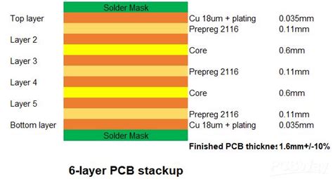
What is the typical thickness of a 6 layer PCB?
The thickness of a 6 layer PCB can vary depending on the materials used and the specific stackup. However, a common thickness range for 6 layer PCBs is between 1.6mm to 2.0mm. -
Can 6 layer PCBs be used for high-frequency applications?
Yes, 6 layer PCBs can be designed to handle high-frequency signals. By carefully selecting the stackup, materials, and design techniques, such as controlled impedance and shielding, 6 layer PCBs can effectively manage high-frequency signals while maintaining signal integrity. -
Are 6 layer PCBs more expensive than 4 layer PCBs?
Yes, 6 layer PCBs are generally more expensive than 4 layer PCBs due to the increased complexity of manufacturing, additional materials required, and the need for more precise processes. However, the cost difference can be justified for applications that require the enhanced performance and functionality offered by 6 layer PCBs. -
How long does it take to manufacture a 6 layer PCB?
The lead time for manufacturing a 6 layer PCB can vary depending on the complexity of the design, the chosen materials, and the workload of the PCB manufacturer. Typically, the lead time ranges from 1 to 3 weeks, but it can be longer for more complex designs or high-volume orders. -
What are the key considerations when designing a 6 layer PCB?
When designing a 6 layer PCB, some key considerations include: - Selecting the appropriate stackup based on signal integrity, power distribution, and EMI requirements.
- Properly managing signal routing, impedance control, and layer transitions.
- Ensuring adequate clearances and spacing between components and traces.
- Considering thermal management and heat dissipation.
- Adhering to manufacturability guidelines and constraints.
Conclusion
6 layer PCBs offer a powerful solution for complex electronic designs that require high component density, improved signal integrity, and efficient power distribution. By understanding the various stackup types and their advantages, designers can select the most suitable configuration for their specific application. Working closely with an experienced 6 layer PCB manufacturer and following best design practices ensures the successful realization of high-quality, reliable, and performance-optimized 6 layer PCBs.
When choosing a 6 layer PCB manufacturer, it is essential to consider factors such as their technical expertise, manufacturing capabilities, quality control processes, and customer support. By partnering with a reputable and experienced manufacturer, you can leverage their knowledge and resources to bring your 6 layer PCB designs to life and achieve the desired functionality and performance for your electronic products.


Leave a Reply