Introduction to Castellated PCB
Printed Circuit Boards (PCBs) are the backbone of modern electronic devices. They provide a platform for mounting and connecting various electronic components to create a functional circuit. One of the most popular methods of assembling PCBs is through the use of Castellated Holes. Castellated PCBs offer numerous advantages over traditional assembly methods, making them an excellent choice for a wide range of applications.
What is a Castellated PCB?
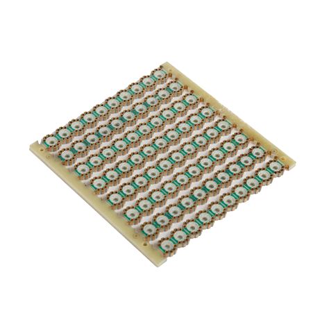
A castellated PCB is a type of printed circuit board that features small, semi-circular holes along its edges. These holes, known as castellations, are plated with a conductive material, typically copper, to allow for electrical connections between the PCB and other components or boards. The term “castellated” comes from the resemblance of these holes to the battlements of a castle wall.
Advantages of Castellated PCBs
Castellated PCBs offer several advantages over traditional assembly methods:
-
Improved Mechanical Strength: The castellated holes provide additional mechanical support, making the PCB more resistant to vibrations and shock.
-
Easier Assembly: Castellated PCBs can be easily soldered to other boards or components using reflow soldering techniques, simplifying the assembly process.
-
Reduced Footprint: By utilizing the edges of the PCB for connections, castellated PCBs can reduce the overall footprint of the assembled board, making them ideal for space-constrained applications.
-
Enhanced Signal Integrity: Castellated holes can help maintain signal integrity by providing shorter, more direct paths for electrical signals.
Designing Castellated PCBs
PCB Layout Considerations
When designing a castellated PCB, several layout considerations must be taken into account:
-
Castellation Dimensions: The size and spacing of the castellated holes should be carefully chosen based on the desired mechanical strength, electrical performance, and manufacturing capabilities.
-
Pad and Trace Sizing: The pads and traces connected to the castellated holes should be appropriately sized to ensure proper soldering and electrical connections.
-
Clearance and Creepage: Sufficient clearance and creepage distances must be maintained between the castellated holes and other conductive features to prevent short circuits and ensure reliable operation.
Manufacturing Considerations
Castellated PCBs require specialized manufacturing processes to ensure the quality and reliability of the final product:
-
Plating: The castellated holes must be plated with a conductive material, typically copper, to enable electrical connections. The plating process should be carefully controlled to ensure uniform coverage and avoid any voids or defects.
-
Drilling: The castellated holes are typically drilled using a specialized drill bit or a laser drilling process. The drilling process must be precise to ensure the holes are correctly sized and positioned.
-
Routing: The PCB panel must be routed or cut to create the individual boards with the castellated edges. The routing process should be carefully controlled to ensure a clean, smooth edge finish.

Assembling Castellated PCBs
Soldering Techniques
Castellated PCBs are typically assembled using reflow soldering techniques:
-
Solder Paste Application: Solder paste is applied to the castellated holes and pads using a stencil or syringe.
-
Component Placement: The components or other boards are placed onto the castellated PCB, with the leads or pads aligned with the castellated holes.
-
Reflow Soldering: The assembled board is subjected to a controlled heating profile in a reflow oven, melting the solder paste and creating a strong mechanical and electrical bond between the components and the PCB.
Inspection and Testing
After assembly, castellated PCBs should undergo thorough inspection and testing to ensure the quality and reliability of the final product:
-
Visual Inspection: The assembled board should be visually inspected for any defects, such as misaligned components, solder bridges, or poor solder joints.
-
Electrical Testing: The assembled board should be subjected to various electrical tests, such as continuity tests, insulation resistance tests, and functional tests, to ensure proper operation and performance.
-
Mechanical Testing: Depending on the application, the assembled board may also need to undergo mechanical tests, such as vibration or shock tests, to ensure its robustness and reliability.

Applications of Castellated PCBs
Castellated PCBs find applications in a wide range of industries and products:
-
Consumer Electronics: Castellated PCBs are commonly used in smartphones, tablets, and wearable devices, where space is at a premium and reliable connections are critical.
-
Industrial Automation: Castellated PCBs are used in industrial control systems, sensors, and actuators, where they must withstand harsh environmental conditions and provide reliable operation.
-
Automotive Electronics: Castellated PCBs are used in various automotive electronic systems, such as engine control units, infotainment systems, and advanced driver assistance systems (ADAS).
-
Medical Devices: Castellated PCBs are used in medical devices, such as implantable devices, diagnostic equipment, and patient monitoring systems, where reliability and miniaturization are essential.

Frequently Asked Questions (FAQ)
1. What is the difference between a castellated PCB and a standard PCB?
A castellated PCB FEAtures small, semi-circular holes along its edges, which are plated with a conductive material to allow for electrical connections. In contrast, a standard PCB does not have these castellated holes and relies on other methods, such as through-hole or surface-mount technology, for making connections.
2. What are the advantages of using castellated PCBs?
Castellated PCBs offer several advantages, including improved mechanical strength, easier assembly, reduced footprint, and enhanced signal integrity. These benefits make them an excellent choice for a wide range of applications, particularly those requiring miniaturization and reliability.
3. How are castellated PCBs manufactured?
The manufacturing process for castellated PCBs involves several specialized steps, including plating the castellated holes with a conductive material, drilling the holes using a specialized drill bit or laser, and routing or cutting the PCB panel to create the individual boards with the castellated edges.
4. What soldering techniques are used for assembling castellated PCBs?
Castellated PCBs are typically assembled using reflow soldering techniques, which involve applying solder paste to the castellated holes and pads, placing the components or other boards onto the PCB, and subjecting the assembled board to a controlled heating profile in a reflow oven to melt the solder and create a strong bond.
5. In what industries are castellated PCBs commonly used?
Castellated PCBs find applications in various industries, including consumer electronics, industrial automation, automotive electronics, and medical devices. They are particularly well-suited for applications requiring miniaturization, reliability, and the ability to withstand harsh environmental conditions.
Conclusion
Castellated PCBs offer a reliable and efficient method for assembling electronic devices, providing numerous advantages over traditional assembly techniques. By understanding the design considerations, manufacturing processes, and assembly techniques involved in creating castellated PCBs, engineers and manufacturers can develop high-quality, reliable products for a wide range of applications. As technology continues to advance and the demand for miniaturized, high-performance electronic devices grows, castellated PCBs will likely play an increasingly important role in shaping the future of the electronics industry.
| Advantage | Description |
|---|---|
| Improved Mechanical Strength | Castellated holes provide additional mechanical support, making the PCB more resistant to vibrations and shock. |
| Easier Assembly | Castellated PCBs can be easily soldered to other boards or components using reflow soldering techniques. |
| Reduced Footprint | By utilizing the edges of the PCB for connections, castellated PCBs can reduce the overall footprint of the assembled board. |
| Enhanced Signal Integrity | Castellated holes can help maintain signal integrity by providing shorter, more direct paths for electrical signals. |


Leave a Reply