The Basics of Circuit Theory
Before you start building actual circuit boards, it’s important to grasp the fundamental concepts that govern how circuits work. Having a solid understanding of circuit theory will help you design boards that function properly and troubleshoot issues when they arise.
Ohm’s Law
One of the most important principles in circuit theory is Ohm’s Law. This law expresses the relationship between voltage (V), current (I), and resistance (R) in a circuit. Mathematically, Ohm’s Law is represented by the equation:
V = I * R
In other words, voltage equals current multiplied by resistance. This means that if you know any two of these values, you can calculate the third.
For example, let’s say you have a 9V battery connected to a 100 ohm resistor. To calculate the current flowing through the resistor, you would use this equation:
I = V / R
I = 9V / 100 ohms
I = 0.09 amps or 90 milliamps
Understanding Ohm’s Law is crucial for properly sizing components like resistors and ensuring your circuit operates within safe voltage and current limits.
Series vs Parallel Circuits
Another key concept to understand is the difference between series and parallel circuits. In a series circuit, components are connected end-to-end in a single loop. In a parallel circuit, components are connected across each other, creating multiple paths for current to flow.
Series circuits have the following properties:
– Voltage drops add up to the source voltage
– Current is the same through all components
– Total resistance is the sum of individual resistances
Parallel circuits have these characteristics:
– Voltage is the same across all components
– Total current is the sum of branch currents
– Total resistance is less than the smallest individual resistance
Many circuits use a combination of series and parallel connections. Being able to recognize and analyze these configurations is an important skill for working with circuit boards.
Capacitance and Inductance
In addition to resistance, capacitance and inductance are two other properties that affect circuit behavior, especially in AC (alternating current) circuits.
Capacitors store electric charge and oppose changes in voltage. They are used for filtering, timing, decoupling, and more. Capacitance (C) is measured in farads (F).
Inductors, made from coils of wire, store energy in a magnetic field and oppose changes in current. They have many applications including filtering, energy storage, and current limiting. Inductance (L) is measured in henries (H).
Understanding how capacitors and inductors work and what role they play in circuits is important for more advanced Circuit board design.
Gathering the Right Tools and Components
With a grasp on basic circuit theory under your belt, you’re ready to start acquiring the tools and components you’ll need to actually start building circuit boards.
Essential Tools
At minimum, you’ll need the following tools to get started:
| Tool | Purpose |
|---|---|
| Soldering iron | Used to melt solder and join components to the circuit board. Look for adjustable temperature control and interchangeable tips. |
| Solder | A metal alloy that melts and forms electrical connections between components. Leaded solder is easier to work with but lead-free is safer. Use thin solder (e.g. 0.8mm) for most applications. |
| Solder wick | A braided wire used to remove excess solder from joints. Also called Desoldering Braid. |
| Wire strippers | A tool used to remove the insulation from the ends of wires prior to soldering. |
| Flush cutters | Used to trim the leads of components after soldering. Also handy for cutting wires to length. |
| Multimeter | A device that measures voltage, current, resistance, and other electrical properties. Essential for testing and troubleshooting circuits. Look for an auto-ranging digital multimeter. |
| Tweezers | Used for handling and positioning small components during soldering. Curved precision tweezers work well. |
| “Helping hands” | A device with adjustable alligator clips that holds the circuit board and components in place while you solder. |
| Safety glasses | Protects your eyes from solder splashes or flying wire trimmings. A must for soldering safety. |
As you progress, you may want to invest in additional tools like a hot air rework station, solder paste stencils, a microscope, etc. But the tools listed above are sufficient for getting started with most through-hole soldering projects.
Choosing Components
The specific components you need will depend on the circuit board project you are working on. However, here are some common components that are used in many projects:
- Resistors
- Capacitors
- Diodes (rectifier, zener, LED, etc.)
- Transistors (BJT, MOSFET, etc.)
- Integrated circuits (microcontrollers, voltage regulators, amplifiers, timers, etc.)
- Connectors and switches
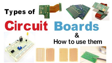
- Prototype board (breadboard, perfboard, etc.)
- Printed circuit board (PCB)
When choosing components for your projects, pay attention to key specifications like resistance, capacitance, voltage/current ratings, package types, etc. to ensure they will work for your application. Referring to component datasheets can help you select parts with the right specifications.
It’s also a good idea to start out with a kit that includes a variety of common components so you have what you need on hand for experimenting and learning. As you gain experience, you can stock up on specific components for the projects you want to build.

Understanding Schematics
Being able to read and draw schematic diagrams is an essential skill for circuit board design. A schematic is a graphical representation of how the components in a circuit are connected together electrically. It uses standardized symbols to represent components and lines to represent the wires connecting them.
Here are some of the most common schematic symbols you should know:
| Symbol | Component |
|---|---|
| Resistor | |
| Capacitor | |
| Diode | |
| Light-emitting diode (LED) | |
| NPN Bipolar Junction Transistor (BJT) | |
| N-channel MOSFET |
In a schematic, components are connected together with lines representing wires. Connections are indicated by a dot where lines intersect. Unconnected crossings of lines are shown with a “hump” in one of the lines.
Power and ground connections are also important in schematics. The power supply is often labeled with +V, Vcc, or Vdd. Ground is indicated by a downward-pointing triangle or “ground” symbol.
Being able to “read” a schematic, to look at the symbols and visualize how the actual components will be wired together, is a skill you’ll develop with practice. And learning to neatly draw your own schematics is important for documenting your designs and communicating them to others.
There are also many software tools available for drawing schematics electronically. Some popular options are KiCad, Eagle, and EasyEDA. Using electronic design automation (EDA) tools allows you to easily draw schematics and convert them into PCB layouts.

PCB Design Basics
Once you have a completed schematic for your circuit, the next step is to design the actual printed circuit board (PCB) that the components will be soldered to. The PCB provides mechanical support for the components and uses conductive copper traces to electrically connect the components as specified in the schematic.
PCB Layers
Most PCBs are made up of multiple layers:
– Silkscreen: The top layer that has component outlines and labels printed on it
– Solder mask: The protective coating that covers the copper traces, with openings for the component pads and vias
– Copper: The conductive layer that forms the traces and pads to connect components. Simple PCBs may have just a single layer of copper, while more complex boards can have multiple layers.
– Substrate: The non-conductive material, typically fiberglass (FR4), that provides structure for the PCB
The copper layer is the most important for the functionality of the board. Traces on the copper layer form the point-to-point connections between components. Vias are copper-plated holes that allow traces to connect from one layer of the board to another.
PCB Layout
Designing the PCB layout translates the information from the schematic to the physical board. The layout process involves:
- Placing components on the board
- Routing traces to connect the components
- Adding copper fills for power and ground
- Defining the board outline
Many EDA tools have an autorouter feature that automatically routes traces between components. However, for best results, traces should be routed manually following good design practices:
- Minimize trace length to reduce resistance and inductance
- Use wide traces for power and ground connections
- Avoid sharp corners in traces to prevent Acid Traps during manufacturing
- Provide adequate clearance between traces to prevent shorts
- Keep sensitive analog traces away from noisy digital traces
- Use ground fills and planes to provide shielding
It’s also important to consider the manufacturability of your PCB design. Most PCB fabrication houses have specific requirements for minimum trace width and spacing, hole sizes, etc. Following your manufacturer’s design rules will ensure your boards can be produced correctly and help minimize cost.

Soldering Techniques
Soldering is the process of using a metal alloy (solder) to join components to the pads on a circuit board. Proper soldering is critical to ensure strong mechanical and electrical connections. Poor soldering can result in unreliable or non-functional boards.
Choosing the Right Solder
Solder is an alloy made primarily of tin, with other metals like lead, silver, or copper added. It comes in both leaded and lead-free varieties. Leaded solder, typically 63% tin/37% lead, melts at a lower temperature and is easier to work with. However, lead is toxic, so lead-free solder is now required for most commercial electronics.
Solder also comes in different thicknesses. For most through-hole soldering, a solder diameter of 0.8mm is a good choice. Thinner solder, down to 0.3mm, is used for surface-mount components.
Flux is an important part of the soldering process. Flux cleans the metal surfaces and helps the solder flow onto the joint. Solder wire has a core of flux – “rosin core” solder is preferred for electronics. You can also use additional flux applied separately to the joint before soldering for improved results.
The Right Soldering Iron
A good soldering iron is essential for quality soldering. Look for these features:
– Adjustable temperature control. Different components and Solder Types require different temperatures. Adjustable temperature lets you fine-tune the heat for the best results.
– Interchangeable tips. Being able to swap tip shapes and sizes is important for soldering different types of components.
– Sufficient wattage. A 40-60 watt soldering iron provides enough heat for most through-hole soldering. Lower wattage irons may struggle with larger joints.
Proper Soldering Technique
Good soldering technique will create a strong, reliable joint and prevent damage to components. Follow these steps:
- Ensure the component leads and PCB pads are clean. If needed, clean with isopropyl alcohol and a brush.
- Apply fresh solder to the tip of the iron to tin it. This helps with heat transfer.
- Touch the tip of the iron to both the component lead and the PCB pad simultaneously.
- Feed solder into the joint opposite the tip of the iron. The solder should melt from the heat of the joint, not from the iron directly.
- Continue feeding solder until the joint is filled and the solder forms a concave fillet shape.
- Remove the solder and then the iron while keeping the joint still. Allow the joint to cool undisturbed.
- Inspect the joint. It should be shiny and smooth, not dull or blobby. The solder should cover the entire pad and fill the hole in the board.
Some other tips:
– Let the iron heat up fully before use
– Avoid touching the iron to the board or component for too long to prevent damage
– Clean the tip frequently on a damp sponge
– Wear safety glasses to prevent eye injury from solder splatter
– Work in a well-ventilated area and avoid breathing solder fumes
Mastering soldering takes practice. Taking the time to perfect your technique will pay off in boards that work reliably. And learning how to desolder and rework joints is also an important skill for fixing mistakes.
Testing and Troubleshooting
With your board assembled, it’s time to apply power and see if it works as intended. Careful testing and methodical troubleshooting are key at this stage.
Visual Inspection
Before powering on your board, give it a thorough visual inspection. Look for:
– Unsoldered pins or joints
– Solder bridges causing shorts between pins or traces
– Reversed or misplaced components
– Damaged or missing components
– Incorrect component values
Catching issues at this stage can prevent further damage when power is applied.
Applying Power
When you’re ready to power on the board for the first time, consider using a current-limited power supply if available. This can prevent damage if there is a short circuit in the board. If a current-limited supply is not available, connect power through a temporary jumper wire so you can quickly disconnect it if needed.
Monitor the board closely on power-up. If you see or smell smoke, or the board gets very hot, disconnect power immediately. This indicates a serious issue like a short or reversed component that will require rework before proceeding.
Testing Functionality
If the board powers up without issue, you can begin testing its functionality. The specifics of this will depend on the board’s purpose. Some things to check:
– Use a multimeter to verify expected voltage levels at the power input and key points throughout the circuit
– Check for signals at the outputs of the board
– Test the response to different inputs
– Verify any peripheral connections like buttons, sensors, displays, etc.
– Probe test points and compare to expected behavior from the schematic
Keeping detailed notes during testing can help with troubleshooting any issues you find.
Logical Troubleshooting
When you encounter a problem with the board’s operation, approach it systematically:
- Clearly define the problem. What is the board doing or not doing?
- Generate a hypothesis for the cause. Based on the schematic and your knowledge of the circuit, what could explain the problem?
- Test your hypothesis. Use a multimeter or oscilloscope to probe key points and see if the circuit is behaving as you expect.
- Narrow it down. Work to isolate the problem to a specific component or section of the board.
- Rework and retest. Make any necessary changes and then retest to see if the problem is resolved.
Some common issues to look out for include:
– Incorrect component values or orientation
– Poor solder joints
– Damaged components
– Shorts or opens on the PCB
– Incorrect power supply voltage or polarity
– Loose or misaligned connectors
– Software or firmware bugs
Taking a logical, step-by-step approach to troubleshooting can make even complex issues manageable. And remember, every problem is a learning opportunity. Figuring out what went wrong and how to fix it will make you a better circuit designer in the long run.
FAQ
To wrap up, let’s address some frequently asked questions about Circuit Board Projects for beginners:
Q: What’s the best way to learn circuit board design?
A: Hands-on practice is key. Start by studying basic circuits and working through kits or tutorials. As you gain confidence, design and build your own simple projects. Analyze circuits you come across and learn from other people’s designs. And don’t be afraid to make mistakes – troubleshooting is a great teacher.
Q: What software should I use for circuit design?
A: There are many options ranging from simple to full-featured. Some popular choices are KiCad, Eagle, EasyEDA, and Fritzing. Many have free versions that are


Leave a Reply