What is PCA Electronics?
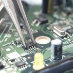
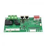
PCA Electronics, short for Printed Circuit Assembly Electronics, refers to the process of assembling various electronic components onto a printed circuit board (PCB) to create a functional electronic device. PCBs are the backbone of modern electronics, providing a platform for components to be mounted and interconnected to form complex circuits. PCA Electronics involves the design, manufacturing, and testing of these assembled PCBs.
Key Components of PCA Electronics
- Printed Circuit Board (PCB)
- Electronic Components (resistors, capacitors, integrated circuits, etc.)
- Solder
- Assembly Equipment (pick-and-place machines, reflow ovens, etc.)
The PCA Electronics Process
The PCA Electronics process can be divided into several stages, each playing a crucial role in the creation of a reliable and functional electronic device.
Step 1: PCB Design
The first step in PCA Electronics is designing the printed circuit board. This involves creating a schematic diagram that outlines the electrical connections between components, followed by a layout design that determines the physical placement of components on the board. PCB design software, such as Altium Designer or Eagle, is commonly used for this purpose.
Step 2: PCB Fabrication
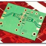
Once the PCB design is finalized, the next step is to fabricate the physical board. This process typically involves the following sub-steps:
- Printing the circuit pattern onto a copper-clad laminate using photoresist and UV light exposure.
- Etching away the unwanted copper, leaving only the desired circuit pattern.
- Drilling holes for through-hole components and vias.
- Applying a solder mask to protect the copper traces and prevent short circuits.
- Adding a silkscreen layer for component labels and other markings.
Step 3: Component Placement
With the fabricated PCB ready, the next stage is to place the electronic components onto the board. This is typically done using automated pick-and-place machines, which can quickly and accurately place hundreds of components per minute. The components are usually supplied on reels or trays and are picked up by the machine using a vacuum nozzle or gripper.
Step 4: Soldering
After the components are placed, they need to be soldered to the PCB to create electrical connections. There are two primary Soldering Methods used in PCA Electronics:
-
Wave Soldering: This method is used for through-hole components. The PCB is passed over a molten solder wave, which wicks up through the holes and creates a connection between the component leads and the PCB pads.
-
Reflow Soldering: This method is used for surface-mount components. A solder paste, containing tiny solder spheres mixed with flux, is applied to the PCB pads using a stencil. The components are then placed onto the solder paste. The entire assembly is heated in a reflow oven, melting the solder and creating a permanent connection.
Step 5: Inspection and Testing
Once the soldering process is complete, the assembled PCBs undergo inspection and testing to ensure quality and functionality. This may include:
- Visual inspection for proper component placement and soldering.
- Automated Optical Inspection (AOI) using cameras and image processing software to detect defects.
- X-ray inspection for hidden solder joints or component issues.
- In-Circuit Testing (ICT) to verify the electrical performance of individual components and circuits.
- Functional testing to ensure the overall device operates as intended.
Step 6: Conformal Coating and Potting
In some cases, additional protection for the assembled PCB may be required, especially for devices that will be exposed to harsh environments. Conformal coating involves applying a thin layer of protective material, such as acrylic, silicone, or polyurethane, over the PCB to protect against moisture, dust, and other contaminants. Potting, on the other hand, involves encapsulating the entire PCB in a solid compound, such as epoxy or silicone, for even greater protection.
Advantages of PCA Electronics
PCA Electronics offers several advantages over traditional point-to-point wiring or breadboard prototyping:
-
Compact Size: PCBs allow for a much more compact design compared to point-to-point wiring, enabling the creation of smaller and more portable devices.
-
Reliability: Soldered connections on a PCB are much more reliable than wire wrap or breadboard connections, reducing the risk of failures due to loose or broken connections.
-
Consistency: Automated assembly processes ensure consistent quality across multiple PCBs, minimizing the risk of human error.
-
High Volume Production: PCA Electronics is well-suited for high-volume production, as automated assembly processes can quickly produce large quantities of identical PCBs.
-
Cost-Effective: For large production runs, PCA Electronics can be more cost-effective than other assembly methods due to the use of automated processes and economies of scale.

Applications of PCA Electronics
PCA Electronics finds applications across a wide range of industries and products, including:
- Consumer Electronics (smartphones, laptops, televisions, etc.)
- Automotive Electronics (engine control units, infotainment systems, sensors, etc.)
- Medical Devices (patient monitors, diagnostic equipment, wearable devices, etc.)
- Industrial Control Systems (PLCs, motor drives, power supplies, etc.)
- Aerospace and Defense (avionics, communication systems, radar, etc.)
- Internet of Things (IoT) Devices (smart home appliances, wearables, sensors, etc.)
Choosing a PCA Electronics Manufacturer
When selecting a PCA Electronics manufacturer, there are several key factors to consider to ensure a successful partnership:
-
Technical Capabilities: Ensure the manufacturer has experience with the specific technologies and components required for your product, as well as the necessary equipment and processes in place.
-
Quality Management: Look for manufacturers with robust quality management systems, such as ISO 9001 certification, and a track record of producing high-quality products.
-
Production Capacity: Consider the manufacturer’s production capacity and lead times to ensure they can meet your volume requirements and deadlines.
-
Supply Chain Management: A reliable manufacturer should have a well-managed supply chain to ensure a steady flow of components and minimize the risk of production delays.
-
Communication and Support: Clear communication and responsive support are essential for a smooth production process. Look for manufacturers that prioritize customer service and are willing to work closely with you to address any issues that may arise.
Future Trends in PCA Electronics
As technology continues to advance, several trends are shaping the future of PCA Electronics:
-
Miniaturization: The demand for smaller, more compact devices is driving the development of advanced packaging technologies, such as System-in-Package (SiP) and 3D integrated circuits.
-
Flexible and Stretchable Electronics: The rise of wearable devices and the Internet of Things (IoT) is leading to the development of flexible and stretchable PCBs that can conform to various shapes and withstand bending and stretching.
-
High-Speed and High-Frequency: As data rates continue to increase, there is a growing need for PCBs that can handle high-speed and high-frequency signals, such as those used in 5G networks and high-performance computing.
-
Sustainable Manufacturing: There is an increasing focus on environmentally-friendly manufacturing practices, such as the use of lead-free solders and the reduction of waste and energy consumption in the production process.
-
Automation and Industry 4.0: The integration of advanced automation, data analytics, and artificial intelligence in the manufacturing process is enabling more efficient, flexible, and intelligent production of PCA Electronics.
FAQ
1. What is the difference between through-hole and surface-mount components?
Through-hole components have leads that are inserted into holes drilled in the PCB and soldered on the opposite side. Surface-mount components are placed directly onto the surface of the PCB and soldered in place. Surface-mount components are generally smaller and better suited for automated assembly.
2. What is the purpose of a solder mask on a PCB?
A solder mask is a layer of polymer applied to the surface of a PCB that serves two main purposes: it protects the copper traces from oxidation and prevents solder bridges from forming between closely spaced pads during the soldering process. The solder mask also provides electrical insulation between components.
3. What is the difference between wave soldering and reflow soldering?
Wave soldering is used for through-hole components, where the PCB is passed over a molten solder wave, allowing the solder to wick up through the holes and create a connection. Reflow soldering is used for surface-mount components, where a solder paste is applied to the PCB pads, and the entire assembly is heated in a reflow oven to melt the solder and create a permanent connection.
4. What is the purpose of conformal coating in PCA Electronics?
Conformal coating is a thin layer of protective material applied over the surface of an assembled PCB to protect it from moisture, dust, chemicals, and other environmental factors that could damage the components or cause short circuits. It is commonly used in devices that will be exposed to harsh environments or require an extra level of protection.
5. How can I ensure the quality of my PCA Electronics products?
To ensure the quality of your PCA Electronics products, work with a reputable manufacturer that has a robust quality management system in place, such as ISO 9001 certification. Implement thorough inspection and testing procedures, including visual inspection, automated optical inspection (AOI), X-ray inspection, in-circuit testing (ICT), and functional testing. Regularly monitor and review the production process to identify and address any issues that may arise.
| Component Type | Placement Method | Soldering Method |
|---|---|---|
| Through-hole | Manual or automated insertion | Wave soldering |
| Surface-mount | Pick-and-place machine | Reflow soldering |
| Inspection Method | Purpose |
|---|---|
| Visual Inspection | Detect visible defects in component placement and soldering |
| Automated Optical Inspection (AOI) | Use cameras and image processing to detect defects |
| X-ray Inspection | Inspect hidden solder joints and component issues |
| In-Circuit Testing (ICT) | Verify electrical performance of individual components and circuits |
| Functional Testing | Ensure the overall device operates as intended |
By understanding the PCA Electronics process, from design and manufacturing to inspection and testing, you can ensure the creation of high-quality, reliable electronic devices that meet the needs of your customers and the demands of the market. Staying informed about the latest trends and technologies in PCA Electronics will help you remain competitive and adapt to the ever-evolving landscape of the electronics industry.

Leave a Reply