Introduction to PCB Manufacturing
Printed Circuit Board (PCB) manufacturing is a complex process that involves several critical steps to ensure the production of high-quality, reliable boards. From design and material selection to fabrication and testing, each stage requires careful consideration and adherence to best practices. This article will explore the key points to note in PCB manufacturing, helping you navigate the process and achieve optimal results.
Importance of PCB Design
Schematic Design
The first step in PCB manufacturing is creating a schematic design. This is a graphical representation of the electronic circuit, showing all components and their interconnections. A well-designed schematic is essential for a successful PCB. Consider the following:
- Use standardized symbols and notation for clarity
- Double-check component values and connections
- Minimize crossing wires and keep the design clean
PCB Layout
Once the schematic is complete, the next step is to create the PCB layout. This involves arranging components and routing traces on the board. Key points to consider:
- Component placement: Group related components together and consider signal flow
- Trace routing: Minimize trace length, avoid sharp angles, and maintain proper spacing
- Ground plane: Use a solid ground plane for better signal integrity and EMI reduction
- Design rule check (DRC): Perform a DRC to ensure the layout meets manufacturing constraints

Material Selection
Choosing the right materials for your PCB is crucial for its performance and reliability. Consider the following factors:
Substrate Material
The substrate is the insulating layer that supports the copper traces. Common materials include:
| Material | Characteristics | Applications |
|---|---|---|
| FR-4 | Low cost, good mechanical strength, suitable for most applications | General-purpose PCBs |
| High Tg FR-4 | Higher glass transition temperature, better thermal stability | Automotive, aerospace |
| Polyimide | High temperature resistance, flexibility | Flexible PCBs, high-reliability applications |
| Teflon | Low dielectric constant, high frequency performance | RF and microwave circuits |
Copper Weight
Copper weight refers to the thickness of the copper layer on the PCB. It is measured in ounces per square foot (oz/ft²). Common copper weights include:
| Copper Weight | Thickness (mm) | Applications |
|---|---|---|
| 0.5 oz/ft² | 0.0175 | Low-current, low-cost PCBs |
| 1 oz/ft² | 0.0350 | General-purpose PCBs |
| 2 oz/ft² | 0.0700 | High-current, power electronics |
| 3 oz/ft² | 0.1050 | Extreme high-current applications |
Choose the appropriate copper weight based on your current carrying requirements and trace width constraints.
Solder Mask and Silkscreen
- Solder mask: A protective layer applied over the copper traces, leaving only exposed pads for soldering. It prevents solder bridges and provides insulation.
- Silkscreen: Text and symbols printed on the PCB for component identification and assembly instructions. Ensure readability and clarity of the silkscreen.

PCB Fabrication Process
PCB Etching
PCB etching is the process of removing unwanted copper from the substrate, leaving only the desired traces. Two common methods are:
- Wet etching: The PCB is immersed in a chemical solution that dissolves the exposed copper. It is a simple and low-cost method but can result in undercutting of traces.
- Dry etching: Uses plasma or laser to remove the copper. It offers better resolution and control but is more expensive.
Drilling and Plating
After etching, holes are drilled in the PCB for component leads and vias. The holes are then plated with copper to provide electrical connection between layers. Consider the following:
- Drill bit size: Choose the appropriate drill bit size for your component leads and vias
- Plating thickness: Ensure sufficient plating thickness for reliable connections
- Aspect ratio: The ratio of hole depth to diameter should be within acceptable limits
Solder Mask Application
The solder mask is applied to the PCB using either silk screening or photoimaging. The process involves:
- Applying the solder mask material
- Exposing the solder mask to UV light through a photomask
- Developing the solder mask to remove unexposed areas
- Curing the solder mask for durability
Surface Finish
The final step in PCB fabrication is applying a surface finish to the exposed copper pads. Common surface finishes include:
| Finish | Characteristics | Applications |
|---|---|---|
| HASL | Hot air solder leveling, low cost, good solderability | General-purpose PCBs |
| ENIG | Electroless nickel immersion gold, flat surface, long shelf life | High-reliability, fine-pitch components |
| OSP | Organic solderability preservative, thin layer, low cost | Short-term storage, quick assembly |
| Immersion Silver | Good solderability, low cost, prone to tarnishing | General-purpose, short-term storage |
Choose the surface finish based on your soldering requirements, shelf life, and budget.

PCB Assembly
Component Placement
Accurate component placement is essential for a successful PCB assembly. Use the following guidelines:
- Pick and place machine: Use an automated pick and place machine for high-volume, high-accuracy placement
- Placement tolerance: Ensure components are placed within the specified tolerance, typically ±0.1mm
- Polarity and orientation: Double-check component polarity and orientation before placement
Soldering
Soldering is the process of forming electrical and mechanical connections between components and the PCB. Two common methods are:
- Wave soldering: The PCB is passed over a wave of molten solder, suitable for through-hole components
- Reflow soldering: Solder paste is applied to the pads, components are placed, and the PCB is heated to melt the solder. Suitable for surface mount components.
Ensure proper solder joint formation, avoid bridging or cold joints, and clean any flux residue after soldering.
PCB Testing and Inspection
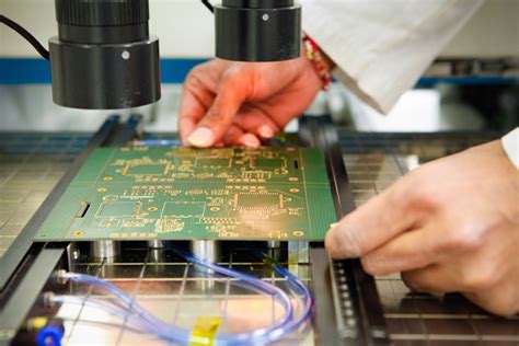
Automated Optical Inspection (AOI)
AOI uses cameras and image processing software to inspect the PCB for defects such as:
- Component placement errors
- Solder joint defects (bridging, insufficient solder)
- Missing or incorrect components
AOI is a fast and efficient method for catching assembly defects early in the process.
In-Circuit Testing (ICT)
ICT uses a bed of nails fixture to make electrical contact with the PCB and test for:
- Short and open circuits
- Component values and tolerances
- Basic functionality
ICT provides a more thorough electrical test than AOI but requires a custom fixture for each PCB design.
Functional Testing
Functional testing involves powering up the PCB and testing its operation in a simulated environment. This can include:
- Boundary scan testing: Using JTAG interface to test interconnects and components
- Firmware programming: Loading and testing the device firmware
- System-level testing: Testing the PCB in the final product or application
Functional testing ensures that the PCB performs as intended in its end-use environment.
Quality Control and Documentation
Statistical Process Control (SPC)
SPC involves monitoring the manufacturing process through statistical methods to ensure consistent quality. Key steps include:
- Defining critical process parameters and tolerance limits
- Collecting and analyzing process data
- Identifying and correcting process deviations
SPC helps maintain a stable and capable manufacturing process, reducing defects and improving yield.
Traceability and Documentation
Maintain a clear record of the PCB manufacturing process, including:
- Material certificates and lot numbers
- Process parameters and settings
- Test results and inspection records
- Serial numbers and date codes of finished PCBs
Good traceability and documentation practices enable faster problem-solving, compliance with regulations, and continuous improvement of the manufacturing process.
Frequently Asked Questions (FAQ)
1. What is the typical turnaround time for PCB manufacturing?
The turnaround time for PCB manufacturing depends on various factors such as the complexity of the design, the chosen fabrication house, and the order quantity. For standard 2-layer PCBs, the turnaround time can be as short as 24 hours for quick-turn prototypes, while more complex designs or larger quantities may take several weeks. It’s essential to communicate your timeline requirements with your manufacturer and plan accordingly.
2. How do I choose the right PCB manufacturer?
When selecting a PCB manufacturer, consider the following factors:
- Capabilities: Ensure the manufacturer can handle your PCB complexity, layer count, and special requirements
- Quality: Look for certifications such as ISO 9001, UL, and IPC standards
- Experience: Choose a manufacturer with a proven track record in your industry or application
- Communication: Clear and responsive communication is essential for a smooth manufacturing process
- Cost: Get quotes from multiple manufacturers and compare pricing, but don’t sacrifice quality for cost
3. What are some common PCB manufacturing defects to watch out for?
Some common PCB manufacturing defects include:
- Solder bridges or insufficient solder on pads
- Drill misalignment or incorrect hole sizes
- Trace width or spacing violations
- Incorrect component placement or orientation
- Contamination or foreign object debris (FOD) on the PCB
Thorough testing and inspection processes can help catch and correct these defects before the PCBs are shipped.
4. How can I minimize the cost of PCB manufacturing?
To minimize the cost of PCB manufacturing, consider the following strategies:
- Optimize your design for manufacturability, avoiding unnecessary complexity
- Use standard materials and components whenever possible
- Panelize multiple PCB designs onto a single panel to reduce fabrication costs
- Order in larger quantities to take advantage of volume discounts
- Choose a cost-effective manufacturer that meets your quality requirements
5. What are some best practices for PCB design and manufacturing?
Some best practices for PCB design and manufacturing include:
- Follow the manufacturer’s design guidelines and constraints
- Use a consistent and clear naming convention for your design files
- Perform thorough design rule checks (DRC) and verify your design before manufacturing
- Communicate clearly with your manufacturer and provide all necessary files and information
- Allow sufficient time for fabrication and assembly, and plan for potential delays or issues
- Test and inspect your PCBs thoroughly to ensure quality and reliability
By following these best practices and selecting a reputable manufacturer, you can ensure a successful PCB manufacturing process and end product.
Conclusion
PCB manufacturing is a complex process that requires careful attention to detail at every stage. By understanding the key points to note in PCB design, material selection, fabrication, assembly, testing, and quality control, you can ensure the production of high-quality, reliable PCBs that meet your requirements. Effective communication with your manufacturer, adherence to best practices, and thorough testing and inspection are essential for a successful PCB manufacturing process.


Leave a Reply