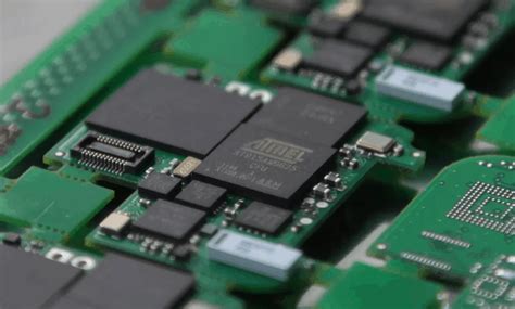
Increased Component Density
One of the most significant advantages of PCB SMT is the ability to achieve higher component density on the circuit board. Surface mount components are much smaller than their through-hole counterparts, allowing for more components to be placed on a single PCB. This increased density enables the design of compact and lightweight electronic devices, which is particularly important in industries such as aerospace, medical devices, and consumer electronics.
Miniaturization of Electronic Devices
The miniaturization of electronic components has been a driving force behind the adoption of SMT. With the ability to place smaller components closer together, designers can create more compact and portable devices. This trend is evident in the evolution of smartphones, wearable technology, and IoT (Internet of Things) devices, where space is at a premium.
Improved Functionality in Limited Space
By accommodating more components on a single PCB, SMT allows for enhanced functionality within a limited space. This means that devices can offer more features and capabilities without increasing their physical size. For example, modern smartphones can incorporate multiple sensors, cameras, and advanced processing power while maintaining a sleek and pocket-friendly form factor.
Enhanced Reliability and Durability
PCB SMT offers superior reliability and durability compared to through-hole mounting. Surface mount components have smaller leads and are directly soldered to the PCB surface, resulting in stronger mechanical bonds and reduced susceptibility to vibration and shock.
Reduced Mechanical Stress
The smaller size and lighter weight of surface mount components put less mechanical stress on the PCB during the assembly process and in the final product. This reduction in stress minimizes the risk of component damage and improves the overall reliability of the electronic device.
Improved Thermal Management
SMT allows for better thermal management due to the smaller size of the components and their direct contact with the PCB surface. The increased surface area contact enables more efficient heat dissipation, preventing overheating and enhancing the long-term reliability of the electronic device.

Faster Assembly and Production
SMT has significantly streamlined the PCB Assembly process, resulting in faster production times and increased efficiency. The use of automated placement machines and reflow soldering techniques enables the rapid assembly of large quantities of PCBs with high precision and consistency.
Automated Placement Machines
SMT assembly heavily relies on automated placement machines, which can accurately place hundreds of components per minute onto the PCB surface. These machines use vision systems and precise motion control to ensure the correct positioning and orientation of each component. The automation of the placement process reduces human error and increases the speed of production.
Reflow Soldering
Reflow soldering is a technique used in SMT where the PCB with pre-placed components is subjected to a controlled heating process. The solder paste, which is applied to the PCB pads, melts and forms a strong bond between the components and the board. Reflow soldering allows for the simultaneous soldering of multiple components, greatly reducing the assembly time compared to manual Soldering Methods.

Cost-Effectiveness
PCB SMT offers several cost advantages over through-hole mounting, making it an attractive option for manufacturers looking to optimize their production costs.
Reduced Material Costs
Surface mount components are generally less expensive than their through-hole counterparts due to their smaller size and simplified packaging. Additionally, SMT requires less PCB real estate, allowing for smaller board sizes and reduced material costs.
Increased Automation and Labor Savings
The highly automated nature of SMT assembly reduces the need for manual labor, resulting in significant cost savings. Automated placement machines and reflow soldering processes minimize the time and resources required for PCB assembly, enabling manufacturers to produce large volumes of PCBs at a lower cost per unit.

Design Flexibility and Innovation
SMT has opened up new possibilities for PCB design and has fostered innovation in the electronics industry. The smaller component sizes and increased density offered by SMT allow for more creative and compact board layouts.
Multi-Layer PCBs
SMT enables the design of multi-layer PCBs, where multiple layers of conductive traces are stacked on top of each other. This allows for more complex routing and increased functionality within a limited space. Multi-layer PCBs are commonly used in high-density applications such as smartphones, tablets, and computer motherboards.
Advanced Packaging Techniques
SMT has paved the way for advanced packaging techniques such as Ball Grid Array (BGA) and Chip Scale Packaging (CSP). These packaging methods offer even higher density and improved electrical performance compared to traditional SMT packages. BGA and CSP are widely used in high-performance applications such as graphics processing units (GPUs) and field-programmable gate arrays (FPGAs).
FAQ
-
Q: What is the difference between SMT and through-hole mounting?
A: SMT involves placing components directly on the surface of the PCB, while through-hole mounting requires components to be inserted through holes in the PCB and soldered on the opposite side. SMT components are smaller and allow for higher density, while through-hole components are larger and provide stronger mechanical connections. -
Q: Can SMT and through-hole components be used together on the same PCB?
A: Yes, it is possible to use both SMT and through-hole components on the same PCB. This is known as a mixed-technology PCB assembly. However, it is important to consider the assembly process and ensure compatibility between the different mounting techniques. -
Q: Are there any disadvantages to using SMT?
A: While SMT offers numerous advantages, there are a few potential drawbacks. SMT components can be more susceptible to moisture and require proper storage and handling. Additionally, the smaller size of SMT components can make manual rework and repair more challenging compared to through-hole components. -
Q: What is the role of solder paste in SMT assembly?
A: Solder paste is a mixture of tiny solder particles suspended in a flux medium. It is applied to the PCB pads prior to component placement. During the reflow soldering process, the solder paste melts and forms a strong electrical and mechanical bond between the components and the PCB. -
Q: How has SMT impacted the electronics industry?
A: SMT has revolutionized the electronics industry by enabling the production of smaller, lighter, and more functionally dense electronic devices. It has allowed for the miniaturization of consumer electronics, the development of advanced packaging techniques, and the increased efficiency and cost-effectiveness of PCB assembly processes.
Conclusion
PCB SMT has transformed the electronics manufacturing landscape, offering numerous advantages over traditional through-hole mounting techniques. From increased component density and miniaturization to enhanced reliability and faster production times, SMT has become the go-to method for PCB assembly.
The benefits of SMT extend beyond just the technical aspects. It has enabled the development of innovative and compact electronic devices that have shaped our modern world. From smartphones and wearables to medical devices and aerospace systems, SMT has played a crucial role in advancing electronics technology.
As the demand for smaller, smarter, and more efficient electronic devices continues to grow, the advantages of PCB SMT will remain relevant and important. Manufacturers and designers who embrace SMT can stay competitive in the market, delivering cutting-edge products that meet the evolving needs of consumers and industries alike.
| Advantage | Description |
|---|---|
| Increased Component Density | SMT allows for higher component density and miniaturization |
| Enhanced Reliability | Stronger mechanical bonds and reduced susceptibility to vibration |
| Faster Assembly | Automated placement machines and reflow soldering enable rapid production |
| Cost-Effectiveness | Reduced material costs and increased automation lead to cost savings |
| Design Flexibility | Smaller component sizes and multi-layer PCBs offer design freedom |
Table 1: Summary of PCB SMT advantages
In conclusion, PCB SMT has proven to be a game-changer in the electronics industry, offering a wide range of advantages that have reshaped the way electronic devices are designed and manufactured. By embracing SMT, companies can achieve higher efficiency, reliability, and innovation in their PCB assembly processes, ultimately delivering better products to consumers.


Leave a Reply