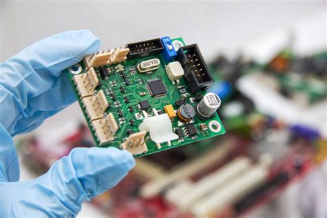
What is PCB Assembly?
PCB assembly is the process of attaching electronic components to a printed circuit board (PCB) to create a functional electronic device. The PCB serves as the foundation for the circuit, providing mechanical support and electrical connectivity for the components. PCB assembly involves several steps, including solder paste application, component placement, reflow soldering, and inspection.
Types of PCB Assembly
There are two main types of PCB assembly: through-hole and surface mount.
-
Through-hole (THT) assembly: In this method, component leads are inserted through holes drilled in the PCB and soldered to pads on the opposite side. THT is an older technology and is typically used for larger components or in applications requiring high mechanical strength.
-
Surface mount technology (SMT) assembly: SMT involves placing components directly onto pads on the PCB surface and soldering them in place. This method allows for smaller components and higher component density, making it the preferred choice for most modern electronic devices.
The PCB Assembly Process
The PCB assembly process consists of several steps that must be carried out in a specific order to ensure a high-quality final product.
Step 1: Solder Paste Application
Solder paste, a mixture of tiny solder particles and flux, is applied to the PCB pads using a stencil or screen printing process. The stencil is a thin metal sheet with openings that correspond to the PCB pads. Solder paste is spread over the stencil, filling the openings and depositing the paste onto the pads.
Step 2: Component Placement
Surface mount components are placed onto the solder paste-coated pads using pick-and-place machines. These machines use computer-controlled nozzles to pick up components from reels or trays and place them accurately on the PCB. For through-hole components, this step is performed manually or with the help of insertion machines.
Step 3: Reflow Soldering
After component placement, the PCB undergoes reflow soldering. The board is passed through a reflow oven, which heats the board according to a specific temperature profile. The solder paste melts, forming a permanent electrical and mechanical bond between the components and the PCB pads. The temperature profile is carefully controlled to ensure proper solder joint formation and to prevent damage to the components.
Step 4: Inspection and Testing
After reflow soldering, the assembled PCB undergoes visual inspection and electrical testing to ensure proper functionality. Automated optical inspection (AOI) systems compare the assembled board to a reference image, identifying any missing or misplaced components, solder bridges, or other defects. Electrical testing verifies that the board functions as intended and meets the specified performance requirements.

PCB Assembly Techniques
Several techniques are used in PCB assembly to ensure high-quality, reliable solder joints and to accommodate different component types and sizes.
Wave Soldering
Wave soldering is used for through-hole components and involves passing the PCB over a molten solder wave. The bottom side of the board is exposed to the solder, which wicks up through the holes and forms solder joints with the component leads. This technique is faster than manual soldering but requires careful control of the solder wave height, temperature, and contact time to ensure consistent results.
Selective Soldering
Selective soldering is a targeted approach used for boards with mixed through-hole and surface mount components. In this process, solder is applied only to specific areas of the board, typically using a mini solder wave or laser soldering system. This technique allows for greater flexibility and reduces the risk of damage to sensitive components.
Hand Soldering
For low-volume production or prototypes, hand soldering may be used. This involves manually applying solder to component leads and PCB pads using a soldering iron. While this method is slower and more labor-intensive than automated techniques, it allows for greater control and can be useful for rework or repair.

PCB Assembly Challenges and Solutions
PCB assembly can present various challenges that must be addressed to ensure a successful outcome.
Moisture Sensitivity
Some components, particularly plastic-encapsulated devices, are sensitive to moisture and can be damaged during reflow soldering if not properly handled. Moisture-sensitive devices (MSDs) should be stored in moisture-barrier bags with desiccants and should be baked before assembly if exposed to ambient conditions for an extended period.
Thermal Management
High-power components generate significant heat during operation, which can lead to reduced performance or failure if not properly managed. Thermal management solutions, such as heatsinks, thermal pads, or fans, can be incorporated into the PCB design to dissipate heat and maintain acceptable operating temperatures.
Electrostatic Discharge (ESD) Protection
Electronic components can be damaged by electrostatic discharge (ESD) during handling and assembly. To prevent ESD damage, PCB assembly should be performed in an ESD-protected environment, using grounded workstations, wrist straps, and ESD-safe materials.

PCB Assembly Testing and Quality Control
To ensure the reliability and performance of assembled PCBs, various testing and quality control measures are employed.
In-Circuit Testing (ICT)
In-circuit testing involves using a bed-of-nails fixture to make electrical contact with test points on the PCB. This allows for individual component testing and can identify faults such as open or short circuits, incorrect component values, or missing components.
Functional Testing
Functional testing verifies that the assembled PCB performs as intended in its final application. This may involve applying power to the board, providing input signals, and measuring output responses to ensure proper functionality.
Boundary Scan Testing
Boundary scan testing, also known as JTAG testing, is a method for testing the interconnections between components on a PCB. This technique uses a serial data path to access and control the boundary pins of compatible components, allowing for the detection of faults such as open or short circuits, stuck-at faults, or incorrect logic states.
PCB Assembly Outsourcing
Many companies choose to outsource PCB assembly to specialized service providers, known as Electronic Manufacturing services (EMS) companies. Outsourcing can offer several advantages, including:
- Access to advanced equipment and expertise
- Reduced capital investment and overhead costs
- Increased production capacity and scalability
- Improved supply chain management
When selecting an EMS partner, consider factors such as their experience, capabilities, quality certifications (e.g., ISO 9001, IPC-A-610), and ability to meet your specific requirements.
PCB Assembly Best Practices
To optimize the PCB assembly process and ensure the best possible results, follow these best practices:
- Design for manufacturability (DFM): Consider the limitations and capabilities of the assembly process during PCB design, such as component spacing, pad sizes, and solder mask clearances.
- Use high-quality materials: Select high-quality PCBs, components, and solder paste to minimize defects and ensure reliable performance.
- Implement proper storage and handling procedures: Store components and PCBs in appropriate conditions (e.g., temperature, humidity) and handle them with care to prevent damage.
- Follow industry standards: Adhere to industry standards such as IPC-A-610 for acceptability criteria and workmanship requirements.
- Regularly maintain and calibrate equipment: Ensure that assembly equipment is properly maintained and calibrated to ensure consistent performance and minimize defects.
Frequently Asked Questions (FAQ)
1. What is the difference between PCB fabrication and PCB assembly?
PCB fabrication is the process of manufacturing the bare printed circuit board, including creating the conductive traces, solder pads, and drilled holes. PCB assembly involves attaching electronic components to the fabricated board to create a functional circuit.
2. What is the advantage of surface mount technology (SMT) over through-hole technology (THT)?
SMT allows for smaller component sizes, higher component density, and automated assembly processes, resulting in smaller, lighter, and more cost-effective PCBs. THT is still used for larger components or in applications requiring higher mechanical strength.
3. How do I select the right solder paste for my PCB assembly?
When choosing a solder paste, consider factors such as the alloy composition (e.g., lead-free or leaded), particle size, flux type (e.g., rosin-based or water-soluble), and viscosity. Consult with your solder paste supplier or EMS provider to select a paste that is compatible with your components and assembly process.
4. What is the purpose of a solder stencil in PCB assembly?
A solder stencil is a thin metal sheet with openings that correspond to the solder pads on a PCB. It is used to apply solder paste to the pads in a precise and consistent manner, ensuring the correct amount of paste is deposited for proper component attachment during reflow soldering.
5. How can I prevent electrostatic discharge (ESD) damage during PCB assembly?
To prevent ESD damage, use an ESD-protected workspace with grounded workstations, wrist straps, and ESD-safe materials. Store components in ESD-safe packaging, and handle PCBs and components with care, avoiding direct contact with exposed pins or leads.
Conclusion
PCB assembly is a critical process in the production of electronic devices, involving the attachment of components to a printed circuit board using various techniques and technologies. By understanding the steps involved, implementing best practices, and addressing common challenges, manufacturers can ensure high-quality, reliable PCB Assemblies that meet the demands of modern electronics applications.


Leave a Reply