Introduction to Reflow soldering
Reflow soldering is a process used in the manufacturing of printed circuit boards (PCBs) to attach surface-mount components to the board. This technique involves applying solder paste to the PCB, placing the components, and then heating the entire assembly to melt the solder and create a strong electrical and mechanical connection. Reflow soldering has become the preferred method for assembling surface-mount devices (SMDs) due to its efficiency, reliability, and compatibility with high-volume production.
Advantages of Reflow Soldering
- High throughput: Reflow soldering allows for the simultaneous soldering of multiple components, making it ideal for mass production.
- Consistency: The automated nature of reflow soldering ensures uniform solder joints across the entire PCB.
- Precision: Reflow soldering enables the accurate placement and soldering of small components, such as chip resistors and capacitors.
- Compatibility: This technique is suitable for a wide range of SMDs and PCB materials.
The Reflow Soldering Process
The reflow soldering process consists of several key steps:
- Solder paste application
- Component placement
- Reflow oven heating
- Cooling and inspection
Step 1: Solder Paste Application
Solder paste is a mixture of tiny solder particles suspended in a flux medium. The paste is applied to the PCB using a stencil printing process or dispensing methods.
Stencil Printing
Stencil printing is the most common method for applying solder paste to PCBs. A stainless steel or polyimide stencil with apertures corresponding to the PCB’s solder pads is aligned with the board. Solder paste is then spread across the stencil using a squeegee, depositing the paste onto the pads through the apertures.
| Stencil Material | Advantages | Disadvantages |
|---|---|---|
| Stainless Steel | Durable, suitable for high-volume production | Expensive, requires regular cleaning |
| Polyimide | Cost-effective, easy to clean | Less durable, limited lifespan |
Dispensing Methods
For low-volume production or prototyping, solder paste can be dispensed using a pneumatic or positive displacement syringe. This method is more time-consuming but offers greater flexibility for custom designs or rework.
Step 2: Component Placement
After applying the solder paste, the surface-mount components are placed onto the PCB. This process can be done manually for small batches or prototypes, but automated pick-and-place machines are used for high-volume production.
Manual Placement
Manual placement involves using tweezers or vacuum pens to position the components on the solder paste. This method is suitable for low-volume production, prototyping, or placing large or odd-shaped components.
Automated Pick-and-Place
Automated pick-and-place machines use computer-controlled nozzles to pick up components from feeders and place them onto the PCB with high precision and speed. These machines can handle a wide range of component sizes and types, making them essential for high-volume production.
Step 3: Reflow Oven Heating
Once the components are placed, the PCB is heated in a reflow oven to melt the solder and form a strong connection between the components and the board. The reflow process follows a specific temperature profile, which consists of four main stages:
- Preheat: The PCB is gradually heated to activate the flux and remove moisture from the solder paste.
- Soak: The temperature is maintained to ensure even heating and flux activation across the board.
- Reflow: The temperature is raised above the solder’s melting point, allowing the solder to flow and form connections between the components and the PCB pads.
- Cool-down: The PCB is cooled to solidify the solder joints.
| Reflow Stage | Temperature Range | Duration |
|---|---|---|
| Preheat | 150-180°C | 60-90 sec |
| Soak | 180-200°C | 60-120 sec |
| Reflow | 220-250°C | 30-60 sec |
| Cool-down | < 100°C | 30-60 sec |
The exact temperature profile depends on the solder paste composition, PCB design, and component characteristics. Manufacturers typically provide recommended profiles for their solder pastes.
Step 4: Cooling and Inspection
After the reflow process, the PCB is cooled to room temperature, allowing the solder joints to solidify. The assembled board is then inspected for defects, such as bridging, tombstoning, or insufficient solder. This inspection can be done visually, using automated optical inspection (AOI) systems, or with X-ray imaging for hidden joints.
Visual Inspection
Visual inspection involves examining the solder joints under magnification to identify defects. This method is suitable for low-volume production or simple PCB designs but can be time-consuming and prone to human error.
Automated Optical Inspection (AOI)
AOI systems use high-resolution cameras and image processing algorithms to detect solder joint defects automatically. These systems can quickly inspect large numbers of PCBs and identify issues that may be difficult to spot visually. AOI is well-suited for high-volume production and complex PCB designs.
X-Ray Inspection
X-ray inspection is used to examine solder joints that are hidden under components, such as ball grid arrays (BGAs) or chip-scale packages (CSPs). This non-destructive method allows for the detection of voids, cracks, or other internal defects that cannot be seen with optical inspection techniques.
Controlling the Reflow Soldering Process
To ensure consistent, high-quality solder joints, several factors must be controlled during the reflow soldering process:
- Solder paste quality
- Stencil design and printing parameters
- Component placement accuracy
- Reflow oven temperature profile
- PCB design and material selection
Solder Paste Quality
Solder paste quality is critical for achieving reliable solder joints. The paste must have the appropriate composition, particle size, and viscosity for the specific application. Proper storage and handling of the solder paste are also essential to maintain its performance.
Stencil Design and Printing Parameters
The stencil design, including aperture size and shape, must be optimized for the PCB layout and solder paste characteristics. Printing parameters, such as squeegee pressure, speed, and angle, should be adjusted to ensure consistent paste deposition.
Component Placement Accuracy
Accurate component placement is essential for proper solder joint formation. Automated pick-and-place machines should be regularly calibrated and maintained to ensure precise component positioning. For manual placement, proper training and ergonomic tools can help improve accuracy and consistency.
Reflow Oven Temperature Profile
The reflow oven temperature profile must be carefully controlled to ensure proper solder melting and flux activation without damaging the components or PCB. Regular oven maintenance and calibration, along with the use of thermocouples or profiling systems, can help maintain the desired temperature profile.
PCB Design and Material Selection
PCB design factors, such as pad size, shape, and spacing, can affect the quality of solder joints. The choice of PCB material, surface finish, and solder mask also influence the reflow soldering process. Designers should follow industry guidelines and collaborate with manufacturing experts to optimize the PCB design for reflow soldering.

Troubleshooting Common Reflow Soldering Defects
Despite careful process control, defects can still occur during reflow soldering. Some common issues include:
- Bridging: Solder connects adjacent pads, creating a short circuit.
- Tombstoning: One end of a component lifts off the pad due to uneven heating or surface tension.
- Insufficient solder: Solder joints are weak or incomplete due to inadequate solder paste volume or poor wetting.
- Solder balls: Small spheres of solder adhere to the PCB surface, potentially causing short circuits.
- Voids: Gaps or bubbles form within the solder joint, reducing its strength and reliability.
To troubleshoot these defects, consider the following actions:
- Review and optimize the solder paste printing process
- Verify the accuracy of component placement
- Adjust the reflow oven temperature profile
- Improve PCB design and pad geometry
- Ensure proper cleaning and maintenance of the production equipment
Best Practices for Reflow Soldering
To achieve consistent, high-quality reflow soldering results, follow these best practices:
- Use high-quality solder paste and store it according to the manufacturer’s recommendations.
- Optimize the stencil design and printing parameters for the specific PCB and components.
- Ensure accurate component placement through machine calibration and operator training.
- Develop and monitor the reflow oven temperature profile using thermocouples or profiling systems.
- Design PCBs with reflow soldering in mind, considering pad size, shape, and spacing.
- Implement a robust inspection and quality control process to identify and address defects quickly.
- Regularly maintain and calibrate production equipment to ensure consistent performance.
- Train operators on best practices and provide ongoing education to keep skills up-to-date.
Frequently Asked Questions (FAQ)
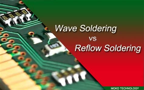
- What is the difference between reflow soldering and wave soldering?
-
Reflow soldering is used for surface-mount components and involves applying solder paste, placing components, and heating the assembly in an oven. Wave soldering is used for through-hole components and involves passing the PCB over a molten solder wave.
-
Can reflow soldering be used for through-hole components?
-
While reflow soldering is primarily used for surface-mount components, it can be used for some through-hole components with special preparation, such as pre-soldering or using Pin-in-Paste techniques.
-
What is the optimal solder paste thickness for reflow soldering?
-
The optimal solder paste thickness depends on the component size and PCB design but typically ranges from 0.1 to 0.2 mm (4 to 8 mils). Consult the solder paste manufacturer’s guidelines and PCB design rules for specific recommendations.
-
How do I select the appropriate reflow oven temperature profile?
-
The reflow oven temperature profile depends on the solder paste composition, PCB design, and component characteristics. Start with the solder paste manufacturer’s recommended profile and adjust as needed based on the specific application and results.
-
What is the shelf life of solder paste, and how should it be stored?
- The shelf life of solder paste varies by manufacturer and composition but typically ranges from 3 to 6 months when stored at room temperature. Solder paste should be stored in a cool, dry place and refrigerated for longer storage periods. Always consult the manufacturer’s storage and handling guidelines.
Conclusion
Reflow soldering is a critical process in the manufacturing of printed circuit boards, enabling the efficient and reliable attachment of surface-mount components. By understanding the key steps involved, controlling essential factors, and implementing best practices, manufacturers can achieve consistent, high-quality solder joints. As electronic devices continue to advance in complexity and miniaturization, mastering reflow soldering techniques will remain crucial for success in the electronics industry.
Leave a Reply