Table of Contents
- Introduction to PCB Design
- PCB Design Workflow
- Schematic Capture
- Component Placement
- PCB Routing
- Design Rule Check (DRC)
- PCB Manufacturability
- PCB Assembly
- Advanced PCB Design Techniques
- PCB-Design-Software“>PCB Design Software
- Frequently Asked Questions (FAQ)
- Conclusion
Introduction to PCB Design
PCB design is a critical step in the development of electronic devices. It involves translating a schematic diagram, which represents the electrical connections between components, into a physical layout that can be manufactured as a printed circuit board. The primary goals of PCB design are to ensure proper connectivity, minimize signal integrity issues, and optimize the board for manufacturability and reliability.
Key Considerations in PCB Design
- Electrical requirements
- Mechanical constraints
- Thermal management
- Signal integrity
- Electromagnetic compatibility (EMC)
- Manufacturing capabilities

PCB Design Workflow
The PCB design process typically follows a structured workflow to ensure a successful outcome. The main stages of the workflow include:
- Schematic capture: Creating a schematic diagram that represents the electrical connections between components.
- Component placement: Arranging the components on the PCB layout in a logical and efficient manner.
- PCB routing: Connecting the components with conductive tracks while adhering to design rules and constraints.
- Design rule check (DRC): Verifying that the PCB layout complies with the specified design rules to ensure manufacturability and reliability.
- Output generation: Generating the necessary files for PCB fabrication and assembly, such as Gerber files, drill files, and bill of materials (BOM).

Schematic Capture
Schematic capture is the first step in the PCB design process. It involves creating a schematic diagram that represents the electrical connections between components. The schematic serves as a blueprint for the PCB layout and provides a clear understanding of the circuit’s functionality.
Best Practices for Schematic Capture
- Use consistent naming conventions for components and nets
- Organize the schematic into logical hierarchies and functional blocks
- Utilize schematic symbols that accurately represent the components
- Add appropriate annotations and comments for clarity
- Perform schematic validation to catch errors early in the design process

Component Placement
Component placement is a crucial step in PCB design, as it directly impacts the routing process and overall board performance. The goal is to arrange the components in a logical and efficient manner while considering factors such as signal integrity, thermal management, and mechanical constraints.
Factors to Consider in Component Placement
- Functional grouping of components
- Signal flow and routing requirements
- Thermal dissipation and heat management
- Mechanical constraints and enclosure dimensions
- Manufacturing and assembly considerations
| Component Type | Placement Considerations |
|---|---|
| Power Components | – Proximity to power input and distribution – Thermal dissipation and cooling requirements |
| High-speed Components | – Minimizing trace lengths and signal integrity issues – Proper grounding and shielding |
| Connectors | – Accessibility and mechanical stability – Clearance for mating connectors |
| Sensitive Components | – Isolation from noise sources – Proper shielding and grounding |
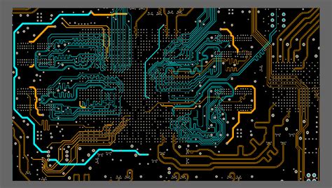
PCB Routing
PCB routing is the process of connecting the components on the board with conductive tracks, known as traces. The objective is to achieve reliable and efficient connections while adhering to design rules and constraints.
Routing Techniques
- Manual routing: Manually placing and editing traces using PCB design software
- Autorouting: Utilizing automated routing algorithms to generate trace paths based on predefined rules and constraints
- Interactive routing: Combining manual and automated routing techniques for optimal results
Routing Considerations
- Trace width and spacing: Ensuring appropriate trace dimensions for current-carrying capacity and manufacturability
- Via placement: Minimizing the number of vias and strategically placing them to improve signal integrity and manufacturability
- Layer stack-up: Selecting the appropriate number and arrangement of layers based on the complexity and requirements of the design
- Impedance control: Maintaining consistent impedance along critical signal paths to minimize reflections and signal distortion
Design Rule Check (DRC)
Design rule check (DRC) is the process of verifying that the PCB layout complies with the specified design rules. These rules ensure that the board can be manufactured reliably and functions as intended.
Common Design Rules
- Minimum trace width and spacing
- Minimum via size and drill diameter
- Clearance between components and traces
- Copper pour and thermal relief settings
- Solder mask and silkscreen requirements
DRC Workflow
- Define the design rules based on the manufacturing capabilities and project requirements
- Run the DRC tool within the PCB design software
- Review and address any rule violations highlighted by the DRC
- Iterate the design and re-run DRC until all violations are resolved
PCB Manufacturability
Designing a PCB with manufacturability in mind is essential to ensure a smooth transition from design to production. Collaborating with the PCB fabrication and assembly partners early in the design process can help identify and address potential manufacturing challenges.
Design for Manufacturability (DFM) Guidelines
- Adhere to the minimum feature sizes and tolerances specified by the PCB fabricator
- Provide adequate clearances and spacing between components and traces
- Use standard via sizes and pad geometries
- Incorporate fiducial markers and tooling holes for automated assembly
- Consider the limitations of the selected PCB fabrication and assembly processes
PCB Assembly
PCB assembly is the process of populating the fabricated PCB with components. It involves soldering the components to the board using various techniques such as through-hole, surface-mount, or mixed assembly.
Assembly Considerations
- Component packaging and footprint compatibility
- Solder paste stencil design and aperture sizes
- Reflow soldering profile and temperature control
- Inspection and testing requirements
- Conformal coating and potting options
Advanced PCB Design Techniques
As PCB designs become more complex and demanding, advanced techniques are employed to address specific challenges and optimize performance.
High-Speed PCB Design
- Signal integrity analysis and simulation
- Impedance matching and termination strategies
- Differential pair routing and length matching
- Crosstalk reduction techniques
RF and Microwave PCB Design
- Controlled impedance transmission lines
- Grounding and shielding techniques
- Cavity resonance mitigation
- Material selection for high-frequency performance
Flexible and Rigid-Flex PCB Design
- Material selection and stack-up considerations
- Bend radius and flexibility requirements
- Strain relief and mechanical support
- Interconnect design and reliability
PCB Design Software
PCB design software plays a vital role in the design and layout process. These tools provide a wide range of features and capabilities to streamline the workflow and ensure accurate and efficient designs.
Popular PCB Design Software
- Altium Designer
- Cadence OrCAD and Allegro
- Mentor Graphics PADS and Xpedition
- KiCad (Open Source)
- Eagle (Autodesk)
Key Features of PCB Design Software
- Schematic capture and component library management
- PCB layout and routing tools
- Design rule checking (DRC) and validation
- 3D visualization and mechanical integration
- Output generation for fabrication and assembly
Frequently Asked Questions (FAQ)
- What is the difference between a schematic and a PCB layout?
-
A schematic represents the electrical connections between components, while a PCB layout is the physical representation of those connections on a printed circuit board.
-
What are the main factors to consider when placing components on a PCB?
-
The main factors to consider include functional grouping, signal flow, thermal management, mechanical constraints, and manufacturing considerations.
-
What is the purpose of design rule check (DRC) in PCB design?
-
DRC ensures that the PCB layout complies with the specified design rules, such as minimum trace width and spacing, to ensure manufacturability and reliability.
-
What are the benefits of using PCB design software?
-
PCB design software streamlines the design process, provides accurate and efficient tools for schematic capture, layout, and routing, and helps ensure design integrity through automated checks and validations.
-
What is the importance of collaborating with PCB fabrication and assembly partners during the design process?
- Collaborating with fabrication and assembly partners helps identify and address potential manufacturing challenges early in the design process, ensuring a smooth transition from design to production.
Conclusion
PCB design and layout is a complex and iterative process that requires a deep understanding of electronic circuits, manufacturing processes, and design principles. By following best practices, utilizing advanced techniques, and leveraging the capabilities of PCB design software, engineers can create reliable, high-performance, and manufacturable PCBs.
As technology continues to evolve, PCB designers must stay up-to-date with the latest tools, techniques, and industry standards to meet the ever-increasing demands of electronic products. By mastering the art and science of PCB design, engineers can bring their innovative ideas to life and contribute to the advancement of the electronics industry.


Leave a Reply