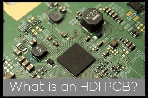
Introduction to HDI PCB
High Density Interconnect (HDI) PCBs are advanced printed circuit boards that offer superior performance and functionality compared to traditional PCBs. HDI PCBs feature finer lines and spaces, smaller vias, and higher connection pad density, enabling the design of more compact and complex electronic devices. As the demand for miniaturization and increased functionality in electronics continues to grow, HDI PCBs have become an essential component in various industries, including telecommunications, consumer electronics, automotive, and medical devices.
What Makes HDI PCBs Different?
HDI PCBs differ from conventional PCBs in several key aspects:
- Finer Lines and Spaces: HDI PCBs have narrower traces and smaller spaces between traces, allowing for higher routing density and more compact designs.
- Smaller Vias: The use of microvias and buried vias in HDI PCBs enables more efficient use of board space and improved signal integrity.
- Higher Connection Pad Density: HDI PCBs accommodate a higher number of connection pads per unit area, facilitating the integration of more components and functions in a smaller footprint.
- Increased Layer Count: HDI PCBs often feature a higher number of layers compared to traditional PCBs, enabling more complex routing and better signal integrity.
Benefits of HDI PCB Technology
Miniaturization and Space Savings
One of the primary advantages of HDI PCBs is their ability to enable miniaturization and space savings in electronic devices. The finer lines, smaller vias, and higher connection pad density allow designers to create more compact and lightweight products without sacrificing functionality or performance. This is particularly important in applications where size and weight are critical factors, such as mobile devices, wearables, and aerospace systems.
Improved Electrical Performance
HDI PCBs offer improved electrical performance compared to traditional PCBs. The shorter signal paths and reduced layer count in HDI designs minimize signal loss, crosstalk, and electromagnetic interference (EMI). Additionally, the use of advanced materials and fabrication techniques in HDI PCBs contributes to better signal integrity and reliability, ensuring optimal performance even in high-speed and high-frequency applications.
Enhanced Functionality and Design Flexibility
The higher routing density and increased layer count in HDI PCBs provide designers with greater flexibility in terms of functionality and design. With HDI technology, it is possible to integrate more features and components into a single board, enabling the development of highly sophisticated and feature-rich electronic devices. This enhanced design flexibility allows for the creation of innovative products that meet the evolving needs of consumers and industries.
Cost Reduction and Faster Time-to-Market
While HDI PCBs may have a higher initial cost compared to traditional PCBs, they can lead to overall cost savings in the long run. The miniaturization and space savings enabled by HDI technology can reduce the size and weight of the final product, resulting in lower material and shipping costs. Additionally, the improved electrical performance and reliability of HDI PCBs can minimize the need for rework and repairs, further reducing costs associated with product failures and warranty claims.
Furthermore, the design flexibility and faster signal propagation in HDI PCBs can accelerate the product development process, allowing for quicker prototyping and shorter time-to-market. This is particularly advantageous in industries where rapid innovation and product launches are essential for staying competitive.

HDI PCB Manufacturing Process
The manufacturing process for HDI PCBs is more complex and demanding than that of traditional PCBs. It involves several specialized techniques and materials to achieve the required level of precision and performance. The following are the key steps in the HDI PCB manufacturing process:
1. Material Selection
The choice of materials is crucial in HDI PCB manufacturing. High-quality, low-loss dielectric materials, such as polyimide and liquid crystal polymer (LCP), are commonly used to ensure optimal signal integrity and reliability. The copper foil used in HDI PCBs is also thinner than that used in traditional PCBs, typically ranging from 0.5 oz to 1 oz per square foot.
2. Lamination
The selected materials are laminated together under high pressure and temperature to form a multilayer stack. In HDI PCBs, the lamination process may involve the use of special techniques, such as Sequential Lamination or build-up lamination, to create the required layer structure and accommodate the high-density interconnects.
3. Drilling and Via Formation
After lamination, the PCB undergoes drilling to create the necessary holes for component mounting and interconnections. In HDI PCBs, microvias and buried vias are formed using specialized laser drilling or photovia processes. These processes allow for the creation of smaller, more precise vias compared to traditional mechanical drilling.
4. Patterning and Etching
The desired circuit pattern is transferred onto the PCB using photolithography and etching processes. In HDI PCBs, the finer lines and spaces require high-resolution imaging and precise etching control to achieve the required accuracy and consistency. Advanced etching techniques, such as plasma etching or laser direct imaging (LDI), may be employed to ensure the quality and reliability of the final product.
5. Surface Finishing
Once the circuit pattern is formed, the PCB undergoes surface finishing to protect the exposed copper and enhance solderability. Common surface finishes used in HDI PCBs include immersion gold (ENIG), electroless nickel/immersion gold (ENEPIG), and organic solderability preservative (OSP). The choice of surface finish depends on the specific application requirements, such as durability, cost, and compatibility with the assembly process.
6. Inspection and Testing
Throughout the manufacturing process, HDI PCBs are subjected to rigorous quality control measures to ensure they meet the required specifications and performance standards. This includes visual inspection, automated optical inspection (AOI), and electrical testing to detect any defects or anomalies. Advanced testing techniques, such as 3D X-ray inspection and thermal stress analysis, may also be employed to validate the reliability and performance of the final product.

HDI PCB Design Considerations
Designing HDI PCBs requires careful consideration of various factors to ensure optimal performance, manufacturability, and reliability. The following are some key design considerations for HDI PCBs:
1. Signal Integrity
Maintaining signal integrity is critical in HDI PCB design. Designers must carefully consider factors such as trace width, spacing, and impedance matching to minimize signal loss, crosstalk, and reflections. Proper grounding and shielding techniques should also be employed to reduce electromagnetic interference (EMI) and ensure stable operation.
2. Thermal Management
The high component density and increased power consumption in HDI PCBs can lead to thermal management challenges. Designers must incorporate adequate heat dissipation mechanisms, such as thermal vias, heatsinks, and cooling fans, to prevent overheating and ensure reliable performance. Thermal simulation and analysis tools can help optimize the thermal design and identify potential hot spots.
3. DFM (Design for Manufacturability)
Designing HDI PCBs with manufacturability in mind is essential for ensuring high yields and reducing production costs. Designers should adhere to the manufacturing capabilities and constraints of the chosen fabrication process, such as minimum feature sizes, via sizes, and layer count limitations. Collaboration with the manufacturing partner early in the design process can help identify and address any potential manufacturability issues.
4. Component Selection and Placement
The selection and placement of components in HDI PCBs require careful consideration to achieve the desired functionality and performance. Designers should choose components that are compatible with the HDI manufacturing process and have appropriate package sizes and pin pitches. The placement of components should be optimized to minimize signal path lengths, reduce crosstalk, and facilitate efficient routing.
5. Testing and Validation
Incorporating testability features into the HDI PCB design can facilitate easier and more efficient testing and validation. This includes the use of test points, boundary scan (JTAG) circuits, and built-in self-test (BIST) functionality. Designers should also consider the accessibility and ease of probing for in-circuit testing and debugging purposes.

Applications of HDI PCB Technology
HDI PCB technology finds applications in a wide range of industries and products. Some of the most common applications include:
1. Consumer Electronics
HDI PCBs are extensively used in consumer electronics, such as smartphones, tablets, laptops, and wearable devices. The miniaturization and increased functionality enabled by HDI technology are essential for creating compact, feature-rich, and high-performance consumer products.
2. Telecommunications
In the telecommunications industry, HDI PCBs are used in various applications, including 5G networks, base stations, routers, and switches. The high-speed and high-frequency capabilities of HDI PCBs are crucial for enabling fast and reliable data transmission in modern communication systems.
3. Automotive Electronics
The automotive industry is increasingly adopting HDI PCB technology for advanced driver assistance systems (ADAS), infotainment systems, and electric vehicle (EV) control units. HDI PCBs offer the necessary reliability, performance, and space savings required for these safety-critical and high-density applications.
4. Medical Devices
HDI PCBs are used in a variety of medical devices, such as implantable devices, diagnostic equipment, and patient monitoring systems. The miniaturization and high reliability of HDI PCBs are essential for creating compact, non-invasive, and highly accurate medical devices that improve patient care and outcomes.
5. Aerospace and Defense
In the aerospace and defense industries, HDI PCBs are used in applications such as avionics, satellite systems, and military communications equipment. The space savings, weight reduction, and high performance offered by HDI technology are critical for meeting the stringent requirements of these demanding applications.
Choosing the Right HDI PCB Manufacturing Partner
Selecting the right HDI PCB manufacturing partner is crucial for ensuring the success of your project. When evaluating potential partners, consider the following factors:
1. Technical Capabilities
Ensure that the manufacturing partner has the necessary technical capabilities and expertise to handle your specific HDI PCB requirements. This includes the ability to accommodate fine lines and spaces, small vias, high layer counts, and advanced materials and processes.
2. Quality and Reliability
Choose a manufacturing partner with a proven track record of delivering high-quality and reliable HDI PCBs. Look for certifications such as ISO 9001, IATF 16949, and AS9100, which demonstrate the partner’s commitment to quality management and continuous improvement.
3. Capacity and Scalability
Consider the manufacturing partner’s production capacity and ability to scale up to meet your current and future needs. A partner with sufficient capacity and flexibility can help you manage demand fluctuations and ensure timely delivery of your products.
4. Cost-Effectiveness
While cost should not be the sole determining factor, it is essential to choose a manufacturing partner that offers competitive pricing without compromising on quality or reliability. Look for partners that offer value-added services, such as design support, prototyping, and supply chain management, which can help optimize your overall costs.
5. Customer Support and Communication
Effective communication and responsive customer support are key to a successful partnership. Choose a manufacturing partner that prioritizes clear and timely communication, provides regular project updates, and offers technical support throughout the product lifecycle.
FAQ
1. What is the difference between HDI PCBs and traditional PCBs?
HDI PCBs differ from traditional PCBs in several key aspects, including finer lines and spaces, smaller vias, higher connection pad density, and increased layer count. These features enable HDI PCBs to offer superior performance, functionality, and miniaturization compared to traditional PCBs.
2. What are the benefits of using HDI PCBs in electronic devices?
The benefits of using HDI PCBs in electronic devices include:
– Miniaturization and space savings
– Improved electrical performance
– Enhanced functionality and design flexibility
– Cost reduction and faster time-to-market
3. What are the key steps in the HDI PCB manufacturing process?
The key steps in the HDI PCB manufacturing process include:
1. Material selection
2. Lamination
3. Drilling and via formation
4. Patterning and etching
5. Surface finishing
6. Inspection and testing
4. What are some important design considerations for HDI PCBs?
When designing HDI PCBs, important considerations include:
– Signal integrity
– Thermal management
– Design for manufacturability (DFM)
– Component selection and placement
– Testing and validation
5. What industries commonly use HDI PCB technology?
HDI PCB technology is commonly used in various industries, including:
– Consumer electronics
– Telecommunications
– Automotive electronics
– Medical devices
– Aerospace and defense
Conclusion
HDI PCB technology has revolutionized the electronics industry, enabling the development of more compact, high-performance, and feature-rich devices. As the demand for miniaturization and increased functionality continues to grow, HDI PCBs have become an essential component in a wide range of applications, from consumer electronics to aerospace and defense.
Choosing the right HDI PCB manufacturing partner is crucial for ensuring the success of your project. By considering factors such as technical capabilities, quality and reliability, capacity and scalability, cost-effectiveness, and customer support, you can select a partner that can help you navigate the complexities of HDI PCB design and manufacturing, and bring your innovative products to market faster and more efficiently.
As technology continues to advance, the importance of HDI PCBs will only continue to grow. By staying up-to-date with the latest developments in HDI PCB technology and partnering with a trusted manufacturing expert, you can position your organization to stay ahead of the curve and deliver cutting-edge electronic devices that meet the evolving needs of your customers and markets.


Leave a Reply