What is ICT PCB?
ICT, or In-Circuit Testing, is a method of testing PCBs by directly probing the individual components on the board. This is done using a specialized test fixture that makes contact with the PCB through a series of pins or probes. The test fixture is connected to a computer-controlled test system that applies a set of electrical tests to each component on the board. These tests are designed to verify that each component is functioning correctly and that the board as a whole meets the required specifications.
How does ICT work?
The ICT process involves several steps:
-
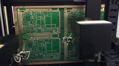
Test fixture design: A custom test fixture is designed for each specific PCB. The fixture consists of a bed of nails that makes contact with the test points on the PCB.
-
Fixture fabrication: The test fixture is fabricated according to the design specifications.
-
PCB loading: The PCB is loaded into the test fixture, ensuring proper alignment and contact with the test probes.
-
Test execution: The test system applies a series of electrical tests to each component on the PCB. These tests typically include:
- Continuity tests: Verifying that there are no open or short circuits on the board.
- Resistance tests: Measuring the resistance of each component and ensuring it falls within the specified range.
- Capacitance tests: Measuring the capacitance of each capacitor and ensuring it meets the required value.
- Inductance tests: Measuring the inductance of each inductor and verifying it meets the specified value.
- Diode tests: Verifying the polarity and forward voltage drop of each diode.
-
Transistor tests: Checking the functionality and gain of each transistor.
-
Results analysis: The test results are analyzed by the test system software, and any defects or discrepancies are flagged for further investigation.
-
Repair and retesting: If any defects are found, the PCB is sent for repair and then retested to ensure the issues have been resolved.
Benefits of ICT PCB
Implementing ICT in your PCB manufacturing process offers several key benefits:
-
Early defect detection: ICT allows you to catch defects early in the manufacturing process, reducing the likelihood of faulty boards reaching the end-user.
-
Reduced manufacturing costs: By identifying defects early, you can avoid the costs associated with rework, scrap, and warranty returns.
-
Improved product quality: ICT ensures that each component on the PCB is functioning correctly, resulting in higher overall product quality.
-
Faster time-to-market: With fewer defects and less need for rework, you can bring your products to market faster.
-
Enhanced customer satisfaction: By delivering high-quality, reliable products, you can improve customer satisfaction and build brand loyalty.

Implementing ICT in Your PCB Manufacturing Process
To effectively implement ICT in your PCB manufacturing process, consider the following steps:
-
Design for testability: When designing your PCB, include test points and other features that facilitate ICT. This may include adding test pads, vias, or connectors that provide access to the components on the board.
-
Select the right test system: Choose an ICT test system that meets your specific requirements in terms of speed, accuracy, and coverage. Consider factors such as the number of test points, the types of components on your board, and the overall complexity of your PCB.
-
Develop comprehensive test coverage: Work with your ICT vendor to develop a comprehensive set of tests that cover all the critical components and functions of your PCB. This may involve creating custom test programs and fixtures tailored to your specific board design.
-
Integrate ICT into your production line: Incorporate ICT into your production line at the appropriate stage, typically after the PCB has been assembled but before final system integration. This allows you to catch defects early and minimize the impact on downstream processes.
-
Continuously monitor and optimize: Regularly review your ICT results and use the data to identify areas for improvement. This may involve fine-tuning your test programs, optimizing your fixture design, or addressing recurring defects in your manufacturing process.

ICT vs. Other PCB Testing Methods
While ICT is a powerful tool for ensuring PCB Quality, it is not the only testing method available. Other common PCB testing methods include:
-
Flying probe testing: A non-contact testing method that uses movable probes to test the PCB. This method is more flexible than ICT but slower and less comprehensive.
-
Boundary scan testing: A testing method that uses built-in test circuitry to test the interconnections between components on the PCB. This method is useful for testing complex boards with high component density.
-
Functional testing: A testing method that verifies the overall functionality of the PCB by simulating real-world operating conditions. This method is typically performed after ICT and before final system integration.
The choice of testing method depends on various factors, including the complexity of the PCB, the types of components used, and the specific quality and reliability requirements of the end product.

Real-world Examples of ICT PCB Success
Many companies across various industries have successfully implemented ICT to improve the quality and reliability of their PCBs. Here are a few examples:
-
Automotive industry: A leading automotive electronics manufacturer implemented ICT to test the PCBs used in its engine control units (ECUs). By catching defects early in the manufacturing process, the company was able to reduce warranty claims and improve overall vehicle reliability.
-
Medical devices: A medical device company used ICT to test the PCBs used in its patient monitoring systems. By ensuring the quality and reliability of these critical components, the company was able to meet the stringent regulatory requirements and ensure patient safety.
-
Aerospace and defense: An aerospace company implemented ICT to test the PCBs used in its satellite communication systems. By identifying and rectifying defects before the systems were deployed, the company was able to avoid costly in-orbit failures and ensure mission success.
These examples demonstrate the versatility and effectiveness of ICT in ensuring PCB quality across a wide range of industries and applications.
FAQ
-
Q: What types of defects can ICT detect?
A: ICT can detect a wide range of defects, including open and short circuits, incorrect component values, missing or misaligned components, and faulty solder joints. -
Q: Can ICT be used to test all types of PCBs?
A: ICT is suitable for testing most types of PCBs, including through-hole and surface-mount designs. However, some complex boards with high component density or unconventional packaging may require additional testing methods. -
Q: How long does ICT take?
A: The duration of an ICT test depends on the complexity of the PCB and the number of test points. Typically, an ICT test can be completed in a matter of seconds to a few minutes per board. -
Q: Is ICT expensive?
A: The initial investment in an ICT system can be substantial, as it requires specialized equipment and custom test fixtures. However, the long-term benefits in terms of improved quality, reduced rework, and faster time-to-market often outweigh the upfront costs. -
Q: Can ICT be performed on prototypes or low-volume production runs?
A: Yes, ICT can be performed on prototypes and low-volume production runs. In fact, performing ICT early in the development process can help identify design issues and ensure the manufacturability of the PCB before committing to high-volume production.
Conclusion
In-Circuit Testing (ICT) is a powerful tool for ensuring the quality and reliability of PCBs in electronics manufacturing. By directly testing the individual components on the board, ICT allows manufacturers to identify and rectify defects early in the production process, reducing costs, improving product quality, and enhancing customer satisfaction.
To successfully implement ICT in your PCB manufacturing process, it is essential to design for testability, select the right test system, develop comprehensive test coverage, integrate ICT into your production line, and continuously monitor and optimize your results.
By leveraging the benefits of ICT and combining it with other testing methods as needed, you can produce high-quality, reliable PCBs that meet the demands of today’s increasingly complex electronic products.
| Testing Method | Advantages | Disadvantages |
|---|---|---|
| ICT | – Comprehensive component-level testing – Fast test execution – Early defect detection |
– Requires custom test fixtures – Higher initial investment – Limited access to some components |
| Flying Probe | – Flexible and adaptable – No custom fixtures required – Suitable for low-volume production |
– Slower test execution – Less comprehensive than ICT – Limited test coverage |
| Boundary Scan | – Tests complex boards with high component density – No physical access to components required – Faster than flying probe testing |
– Requires built-in test circuitry – Limited to digital components – Higher design complexity |
| Functional Testing | – Verifies overall board functionality – Simulates real-world operating conditions – Detects issues not caught by other methods |
– Performed later in the production process – Longer test execution time – Requires custom test software and hardware |
By understanding the strengths and limitations of each testing method and applying them appropriately, you can create a robust testing strategy that ensures the quality and reliability of your PCBs throughout the manufacturing process.


Leave a Reply