Introduction to Solder Mask
Solder mask, also known as solder resist or solder stop mask, is a thin layer of polymer that is applied to the surface of a printed circuit board (PCB) to protect the copper traces from oxidation, corrosion, and short circuits during the soldering process. This protective layer is essential for ensuring the reliability and longevity of electronic devices.
What is a Solder Mask?
A solder mask is a liquid photoimageable coating that is applied to the copper traces of a PCB. It is typically green in color, although other colors such as red, blue, black, and white are also available. The solder mask is applied using a silkscreen printing process or a photo imaging process, depending on the complexity of the PCB design.
Functions of Solder Mask
The primary functions of solder mask are:
-
Protection: Solder mask protects the copper traces from oxidation, corrosion, and mechanical damage during the soldering process and throughout the life of the PCB.
-
Insulation: Solder mask acts as an insulating layer between the copper traces, preventing short circuits and ensuring proper electrical functionality.
-
Aesthetics: Solder mask provides a professional and finished look to the PCB, enhancing its visual appeal.
Types of Solder Mask
There are two main types of solder mask: liquid photoimageable (LPI) and dry film.
Liquid Photoimageable (LPI) Solder Mask
LPI solder mask is a liquid polymer that is applied to the PCB using a silkscreen printing process or a Curtain Coating process. After application, the solder mask is exposed to UV light through a photomask, which hardens the exposed areas while leaving the unexposed areas soluble. The soluble areas are then removed using a developer solution, revealing the copper traces that need to be soldered.
Advantages of LPI solder mask:
– High resolution and accuracy
– Suitable for complex PCB designs
– Excellent adhesion to the copper surface
– Good chemical and thermal resistance
Dry Film Solder Mask
Dry film solder mask is a solid photopolymer film that is laminated onto the PCB surface using heat and pressure. The film is then exposed to UV light through a photomask, which crosslinks the exposed areas while leaving the unexposed areas soluble. The soluble areas are removed using a developer solution, revealing the copper traces.
Advantages of dry film solder mask:
– Faster application process compared to LPI
– Consistent thickness across the PCB surface
– Suitable for high-volume production
– Good chemical and thermal resistance

Solder Mask Application Process
The solder mask application process varies depending on the type of solder mask used and the complexity of the PCB design. However, the general steps involved are as follows:
-
Surface Preparation: The PCB surface is cleaned and treated to ensure proper adhesion of the solder mask.
-
Solder Mask Application: The solder mask is applied to the PCB surface using a silkscreen printing process, curtain coating process, or lamination process.
-
Exposure: The solder mask is exposed to UV light through a photomask, which crosslinks or hardens the exposed areas while leaving the unexposed areas soluble.
-
Development: The soluble areas of the solder mask are removed using a developer solution, revealing the copper traces that need to be soldered.
-
Curing: The solder mask is cured using heat to improve its chemical and thermal resistance properties.
-
Inspection: The PCB is inspected for defects and conformance to the design specifications.

Solder Mask Properties
The properties of solder mask are critical for ensuring the reliability and longevity of electronic devices. Some of the key properties of solder mask include:
Adhesion
Solder mask must have excellent adhesion to the copper surface to prevent delamination during the soldering process and throughout the life of the PCB. Good adhesion ensures that the solder mask remains intact and continues to protect the copper traces from oxidation and corrosion.
Chemical Resistance
Solder mask must be resistant to a wide range of chemicals, including flux, cleaning agents, and other substances used in the manufacturing process. Chemical resistance ensures that the solder mask does not degrade or lose its protective properties over time.
Thermal Resistance
Solder mask must be able to withstand high temperatures during the soldering process without degrading or losing its protective properties. Thermal resistance ensures that the solder mask remains intact and continues to protect the copper traces even under harsh operating conditions.
Electrical Insulation
Solder mask must have excellent electrical insulation properties to prevent short circuits between the copper traces. High electrical insulation ensures that the PCB functions properly and reliably over its entire lifespan.
Flexibility
Solder mask must be flexible enough to withstand the stresses and strains associated with PCB Assembly and use. Good flexibility ensures that the solder mask does not crack or peel off the PCB surface, even under repeated thermal cycling and mechanical stress.

Solder Mask Color Options
Solder mask is available in a variety of colors, each with its own unique properties and applications. Some of the most common solder mask colors include:
| Color | Properties |
|---|---|
| Green | Most common color, provides good contrast for component placement |
| Red | High visibility, often used for power and ground planes |
| Blue | High contrast, often used for high-density PCBs |
| Black | Provides a sleek and professional appearance |
| White | Reflective, often used for LED lighting applications |
The choice of solder mask color depends on the specific application and design requirements of the PCB. For example, green solder mask is often used for general-purpose PCBs, while red solder mask is preferred for power and ground planes due to its high visibility.
Benefits of Using Solder Mask
Using solder mask in PCB manufacturing offers several benefits, including:
-
Improved Reliability: Solder mask protects the copper traces from oxidation, corrosion, and mechanical damage, ensuring the long-term reliability of the PCB.
-
Enhanced Electrical Performance: Solder mask provides excellent electrical insulation between the copper traces, preventing short circuits and ensuring proper electrical functionality.
-
Increased Manufacturing Efficiency: Solder mask simplifies the soldering process by preventing solder bridges and ensuring consistent solder joint formation.
-
Better Aesthetics: Solder mask provides a professional and finished appearance to the PCB, enhancing its visual appeal and brand recognition.
-
Cost Savings: Solder mask reduces the risk of manufacturing defects and rework, leading to cost savings in the long run.
Solder Mask Design Considerations
When designing a PCB with solder mask, several factors must be taken into consideration to ensure optimal performance and reliability. Some of the key design considerations include:
-
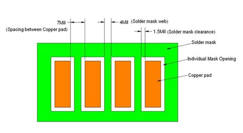
Solder Mask Clearance: Adequate clearance must be provided between the solder mask and the copper traces to prevent solder bridging and ensure proper solder joint formation.
-
Solder Mask Thickness: The thickness of the solder mask must be carefully controlled to ensure consistent coverage and protection of the copper traces.
-
Solder Mask Aperture Size: The size of the solder mask apertures must be carefully designed to ensure proper solder joint formation and prevent solder bridging.
-
Solder Mask Color Selection: The choice of solder mask color must be based on the specific application and design requirements of the PCB.
-
Solder Mask Compatibility: The solder mask must be compatible with the PCB substrate material and the soldering process to ensure optimal performance and reliability.
Common Solder Mask Defects
Despite the many benefits of using solder mask in PCB manufacturing, several defects can occur during the application process. Some of the most common solder mask defects include:
-
Pinholes: Small holes in the solder mask that expose the underlying copper traces, leading to oxidation and corrosion.
-
Solder Mask Residue: Incomplete removal of the soluble areas of the solder mask, leading to poor solder joint formation and reduced reliability.
-
Solder Mask Delamination: Separation of the solder mask from the copper surface, leading to reduced protection and reliability.
-
Solder Mask Cracking: Cracks in the solder mask caused by excessive stress or improper curing, leading to reduced protection and reliability.
-
Solder Mask Misregistration: Misalignment of the solder mask with respect to the copper traces, leading to exposed copper and reduced reliability.
To minimize the occurrence of these defects, careful process control and quality assurance measures must be implemented throughout the solder mask application process.
Frequently Asked Questions (FAQ)
-
Q: What is the purpose of solder mask in PCB manufacturing?
A: The purpose of solder mask is to protect the copper traces from oxidation, corrosion, and short circuits during the soldering process and throughout the life of the PCB. -
Q: What are the two main types of solder mask?
A: The two main types of solder mask are liquid photoimageable (LPI) and dry film solder mask. -
Q: What are some of the key properties of solder mask?
A: Some of the key properties of solder mask include adhesion, chemical resistance, thermal resistance, electrical insulation, and flexibility. -
Q: What are some of the most common solder mask colors?
A: Some of the most common solder mask colors include green, red, blue, black, and white. -
Q: What are some of the most common solder mask defects?
A: Some of the most common solder mask defects include pinholes, solder mask residue, solder mask delamination, solder mask cracking, and solder mask misregistration.
Conclusion
Solder mask is a critical component of PCB manufacturing that provides essential protection and insulation for the copper traces. By understanding the types, properties, and application process of solder mask, PCB designers and manufacturers can ensure optimal performance and reliability of their electronic devices.
Through careful design considerations and process control, the benefits of using solder mask can be maximized while minimizing the occurrence of common defects. As technology continues to advance, the importance of solder mask in PCB manufacturing will only continue to grow, making it an essential area of focus for the electronics industry.


Leave a Reply