What is PCB Tenting?
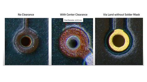
PCB (printed circuit board) tenting is a process where solder mask material is applied over drilled via holes on the PCB instead of around them. This “tents” or covers the hole, creating a flat surface on the PCB. The via hole is still there under the solder mask tent.
Tenting Vias provides several benefits:
– Creates a flat, level surface for better component placement and soldering
– Prevents solder from flowing into the via holes during reflow
– Protects vias from contamination
– Improves PCB strength and durability
– Allows traces to be run between Tented Vias without shorting
Not all vias need to be tented. Typically only smaller vias used for connecting inner layers are tented. Larger vias for through-hole components or that will be used as test points are not tented.
The PCB Manufacturing Process
To understand the importance of PCB tenting, it’s helpful to review the overall PCB manufacturing process:
-
Design: The PCB layout and design is created using EDA (electronic design automation) software. Component placement, routing, drill holes, solder mask, silkscreen, and other features are specified.
-
Printing: The PCB design is printed onto a transparent film or directly onto the copper-clad laminate material.
-
Etching: The printed PCB panels are chemically etched to remove unwanted copper, leaving only the desired copper traces. Multilayer boards have additional steps to laminate the multiple etched layers together.
-
Drilling: All the via holes and component holes are drilled through the PCB panel. Smaller via holes are typically laser drilled while larger holes are mechanically drilled.
-
Plating: The holes are lined with copper to electrically connect the inner layers, making them conductive. Additional copper is plated onto the outer layer traces to the specified thickness.
-
Solder Mask Application: A protective solder mask coating is applied to the outer layers of the PCB. Openings are left in the solder mask for component pads, exposed vias, contact fingers, and other features. At this stage, certain drilled via holes are tented with the solder mask while others are not.
-
Silkscreen: The reference designators, component outlines, and other text markings are printed onto the solder mask in silkscreen. This is typically done in white ink.
-
Surface Finish: A surface finish, such as HASL, lead-free HASL, ENIG, or Immersion Silver, is applied to the exposed copper surfaces to protect them from oxidation and facilitate soldering.
-
Fabrication: The PCB panels are cut into individual boards, and additional fabrication like routing, scoring, beveling may be done. The PCBs are electrically tested and inspected before packaging.
So in summary, PCB tenting occurs at the solder mask application stage, after the vias have been drilled but before the silkscreen and final surface finish. Deciding which vias to tent is an important design consideration.

Advantages of Tenting Vias
Tenting vias offers several key benefits in PCB design and manufacturing:
Prevents Solder Wicking
One of the most important reasons to tent vias is to prevent the solder from flowing into the via holes during component soldering or reflow. This unwanted flow of solder is called solder wicking.
When a via is not tented, the hole can act as a capillary, drawing molten solder off of the component pad and into the via hole through capillary action. This results in too little solder on the component pad and a poor solder joint. It can even cause the component not to be soldered to the pad at all (tombstoning).
By tenting the via with solder mask, the hole is covered and solder is prevented from flowing into it. The solder stays on the component pad where it is needed to form a proper solder joint.
Allows Traces Between Vias
On dense PCB designs, tenting certain vias allows copper traces to be routed between them without short circuiting. If the vias were not tented, the exposed metal in the hole would cause a short circuit if a trace passed over it.
With tenting, since the hole is insulated with solder mask, traces can safely pass between vias. This provides more PCB routing area and greater design flexibility. It can make the difference between routing a dense design on a 4-layer board instead of having to jump up to a 6-layer board.
Protects Against Contamination
Tenting also seals via holes to protect them from contamination. Open vias can collect dirt, dust, Solder Flux residue, and other contaminants during the assembly, soldering, and cleaning processes.
These contaminants can degrade the electrical and mechanical performance of the PCB over time, especially if they are conductive. In severe cases, contamination buildup in via barrels can even cause short circuits.
By sealing the holes with solder mask tenting, contaminants are prevented from collecting inside. Only clean solder mask material covers the openings.
Improves Mechanical Strength
Tenting improves the mechanical strength and durability of PCBs as well. Unfilled vias are essentially just holes in the board, which can weaken its structure. A grid of untented vias across a PCB creates many points of stress and mechanical weakness.
The solder mask tenting helps “glue” the PCB together and reinforce these holes. This strengthens the board and makes it more resistant to flexing, vibration, impacts, and other mechanical stresses. Tented vias are much less likely to cause cracks in solder joints or the PCB itself.
Provides a Flat Surface
Finally, tenting results in a flat, planar surface across the PCB. Untented vias leave dimples or depressions where the holes are.
A planar surface is important for automated pick-and-place assembly equipment. It allows vacuum nozzles to make a better seal for picking up components. It also provides a flat landing zone for placing components accurately.
For surface mount devices with a large number of conductive pads or balls, such as BGAs, the flat surface is critical. If there are untented vias under the device, some balls can fall into the holes and not make proper contact with their pads. A flat, tented surface lets all balls make solid contact.

Disadvantages of Tenting Vias
While tenting has many benefits, there are a few potential disadvantages to consider as well:
Impairs Manual Soldering
One downside of tenting is that it can make manual hand soldering more difficult. With an untented via, the hole provides a path for the soldering iron tip to transfer heat into the joint. The solder flows easily into the via and forms a strong joint.
When a via is tented, the soldering iron can’t make direct contact with the metal in the hole. The solder mask material acts as a thermal insulator, requiring higher temperatures or longer dwell times to solder properly.
Highly skilled manual soldering technicians can usually compensate for this, but it may increase the risk of cold solder joints or damage to the PCB for less experienced assemblers.
Complicates Inspection and Rework
Tented vias can also complicate visual inspection and rework of solder joints. With normal untented vias, inspectors can clearly see the solder fillet flowing into the via, which is a sign of a good solder joint.
With tenting, the solder joint in the via is hidden under the opaque solder mask layer. This makes it more difficult to inspect the joint quality visually. Automated x-ray inspection may be required for critical tented joints.
If a tented joint does need to be reworked, the tented via can impair heat transfer and make it harder to melt the old solder cleanly. There is also a risk of damaging the solder mask tent and exposing the raw via hole.
May Require Thicker Solder Mask
To properly tent vias, the solder mask layer may need to be thicker than normal. The solder mask needs to completely fill and cover the via holes, without any pinholes or voids.
Smaller via holes, in the range of 4-8 mils, can usually be tented with a normal 1mil thick solder mask. However, larger vias up to 20 mil may require a 2-3 mil thick solder mask to tent properly.
The thicker the solder mask is, the more it will interfere with soldering and impact the transfer of heat into joints. Smaller via spans will have less solder mask webbing between the holes, so they can be tented more reliably.
Not Suitable for All Vias
Vias that will be used as test points or will have through-hole components soldered into them cannot be tented. They need to remain open to allow probing and soldering.
Most designs will have a mix of tented and untented vias. The designer needs to specify which vias should be tented and which should not. Typically, only small vias that are used to connect inner layers are tented, while larger vias for test points and component pins are left open.

PCB Layout Guidelines for Tenting
To ensure reliable tenting of vias, PCB designers should follow some layout guidelines and discuss the capability with their fabricator:
- Check Fab Capabilities: Consult with the PCB manufacturer on their capabilities and guidelines for via tenting. Verify they can tent the required via sizes at the desired spacing.
- Limit Tented Via Size: Try to keep tented vias under 20 mils in size. Smaller vias in the range of 4-8 mils are ideal for reliable tenting. Avoid tenting vias larger than 20-25 mils.
- Provide Spacing: Make sure there is adequate solder mask webbing between tented vias. A minimum of 4 mils of solder mask between vias is a good rule of thumb. Larger spacing is even better.
- Specify Tenting in Gerbers: In the CAM/Gerber files provided to the fab house, specify which vias should be tented and which should not. Communicate this clearly to avoid mistakes.
- Consider Thicker Solder Mask: If tenting larger vias up to 20 mils, consider specifying a thicker 2-3 mil solder mask. This will help ensure proper tenting without pinholes.
- Avoid Tenting Pads: Do not tent vias that have component pads or that will be used for test points or socketable pins. The solder mask can impair assembly and testing of these vias.
- Use Smallest Vias Possible: In general, use the smallest via size that is feasible for the design. Smaller vias are easier to tent and take up less routing space on the PCB. 0.006″ to 0.010″ finished hole sizes are common for tenting.
By following these guidelines, designers can create PCB layouts that allow for reliable, high-quality tenting of vias by the fabricator. Clear communication between the designer and manufacturer is key.
Frequently Asked Questions (FAQ)
What is the difference between tented and untented vias?
Tented vias have a layer of solder mask covering the hole opening on the surface of the PCB, while untented vias leave the hole exposed. Tenting helps prevent solder wicking and contamination in via barrels.
Do tented vias make the PCB more expensive?
No, tenting vias does not typically add cost to PCB fabrication. The same solder mask layer is applied as with untented vias. If a thicker solder mask is required to tent larger holes, there may be a slight cost adder.
What is the maximum via size that can be tented?
In general, via holes under 20 mils can be tented reliably. Vias between 20-25 mils may be possible to tent but will likely require a thicker solder mask layer. Consult with the PCB fabricator on their specific capabilities.
How much space is needed between tented vias?
There should be a minimum of 4 mils of solder mask webbing between adjacent tented vias. More space is better for reliable tenting. Consult the manufacturer for their specific design rules and capabilities.
Can vias under BGA pads be tented?
Yes, vias under BGA pads are commonly tented. This provides a flat surface for the BGA balls to collapse onto and make reliable connections to the pads. Untented vias can cause opens if balls fall into the holes.
Conclusion
In summary, tenting of vias is an important technique in PCB design and manufacturing. By covering selected via holes with solder mask, tenting provides several key benefits:
- Prevents solder wicking into via barrels
- Allows traces to be routed between vias
- Protects vias from contamination
- Improves mechanical strength of the PCB
- Provides a flat surface for component placement
While there are some potential disadvantages of tenting, such as difficulty for manual soldering and inspection, these are outweighed by the benefits in most cases.
By understanding the importance of via tenting and following proper PCB layout guidelines, designers can create manufacturable, reliable and cost-effective PCBs. As with any design decision, it’s important to consult with your fabricator on their specific capabilities and guidelines for via tenting.


Leave a Reply