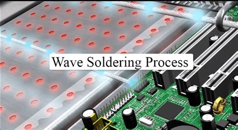
What is Wave Soldering?
Wave soldering is a bulk soldering process used in the manufacture of printed circuit boards (PCBs). The process involves applying a wave of molten solder to the bottom side of a PCB to create electrical connections between components and the board. Wave soldering is an efficient and cost-effective method for soldering high volumes of PCBs, making it a popular choice in the electronics industry.
Advantages of Wave Soldering
- High-speed process suitable for mass production
- Uniform and reliable solder connections
- Cost-effective for large-scale manufacturing
- Suitable for both through-hole and surface mount components
Disadvantages of Wave Soldering
- Not ideal for delicate or heat-sensitive components
- Requires careful setup and maintenance of the soldering equipment
- May require additional cleaning steps post-soldering
The Wave Soldering Process
The wave soldering process consists of several key steps:
- PCB Preparation
- Flux Application
- Preheating
- Solder Wave Contact
- Cooling
- Cleaning and Inspection
1. PCB Preparation
Before wave soldering, the PCB must be properly prepared:
- Components are placed on the top side of the board
- The board is secured to a carrier or pallet to ensure stability during the soldering process
- Solder masks and other protective coatings are applied to areas that should not be soldered
2. Flux Application
Flux is applied to the bottom side of the PCB to remove oxides, prevent re-oxidation, and promote solder wetting.
| Flux Type | Characteristics | Cleaning Required |
|---|---|---|
| Rosin | Mild activation, non-corrosive | Yes |
| Water-Soluble | High activity, corrosive residues | Yes |
| No-Clean | Low residue, non-corrosive | No |
3. Preheating
The PCB is preheated to activate the flux and reduce thermal shock when it contacts the molten solder wave. Preheating is typically done using convection heaters or infrared lamps.
| Preheating Method | Advantages | Disadvantages |
|---|---|---|
| Convection | Even heating, suitable for large PCBs | Slower than infrared |
| Infrared | Fast heating, energy-efficient | Uneven heating, shadow effect |
4. Solder Wave Contact
The preheated PCB is brought into contact with the molten solder wave. The solder wave consists of two parts:
- Chip Wave: A turbulent wave that ensures solder penetration into through-holes and around component leads.
- Lambda Wave: A smooth, laminar wave that helps to remove excess solder and create a clean, even solder joint.
The contact time between the PCB and the solder wave is carefully controlled to ensure optimal solder joint formation.
5. Cooling
After passing through the solder wave, the PCB is cooled to allow the solder joints to solidify. Cooling can be done using air knives or a controlled cooling zone.
6. Cleaning and Inspection
If a no-clean flux is used, the PCB may not require additional cleaning. However, if rosin or water-soluble fluxes are used, the PCB must be cleaned to remove flux residues. Cleaning methods include:
- Solvent cleaning
- Aqueous cleaning
- Ultrasonic cleaning
After cleaning, the PCB undergoes visual inspection and electrical testing to ensure the quality of the solder joints and the overall functionality of the board.

Factors Affecting Wave Soldering Quality
Several factors can impact the quality of wave soldered PCBs:
- Solder composition
- Solder temperature
- Conveyor speed
- PCB design
- Component placement
1. Solder Composition
The most common solder alloys used in wave soldering are tin-lead (SnPb) and lead-free (e.g., SAC305). The choice of solder alloy depends on the specific application and the environmental regulations in the region of manufacture.
| Solder Alloy | Composition | Melting Point (°C) |
|---|---|---|
| SnPb | 63% Sn, 37% Pb | 183 |
| SAC305 | 96.5% Sn, 3% Ag, 0.5% Cu | 217-220 |
2. Solder Temperature
The temperature of the molten solder should be carefully controlled to ensure optimal solder joint formation. The ideal temperature range depends on the solder alloy used:
- SnPb: 200-250°C
- Lead-free: 250-260°C
Excessive solder temperatures can cause thermal damage to components and the PCB, while insufficient temperatures may result in poor solder wetting and weak joints.
3. Conveyor Speed
The speed at which the PCB passes through the solder wave affects the contact time and, consequently, the quality of the solder joints. Optimal conveyor speeds depend on factors such as PCB thickness, component density, and solder alloy.
Typical conveyor speeds range from 1.0 to 2.5 meters per minute. Faster speeds may result in insufficient solder wetting, while slower speeds can cause bridging and excessive solder buildup.
4. PCB Design
The design of the PCB can significantly impact the success of the wave soldering process. Design considerations include:
- Proper component spacing and orientation
- Adequate pad sizes and shapes
- Proper placement of solder thieves and thermal relief pads
- Minimizing differences in thermal mass across the board
5. Component Placement
The placement of components on the PCB can affect the wave soldering process. Key considerations include:
- Ensuring components are securely placed and aligned
- Avoiding shadowing effects, where larger components block solder access to smaller components
- Proper orientation of polarized components
- Use of adhesives or clinching to hold components in place during soldering

Troubleshooting Wave Soldering Defects
Despite careful process control, wave soldering defects can occur. Common defects and their causes include:
| Defect | Cause |
|---|---|
| Bridging | Excessive solder, incorrect conveyor speed, inadequate flux |
| Insufficient Solder | Low solder temperature, inadequate flux, contaminated solder |
| Solder Balls | Excessive flux, contaminated solder, incorrect preheat temperature |
| Lifted Components | Insufficient flux, incorrect component placement, thermal shock |
To minimize defects, regularly monitor and maintain the wave soldering equipment, ensure proper PCB design and component placement, and optimize process parameters such as solder temperature, conveyor speed, and flux application.

Frequently Asked Questions (FAQ)
- What is the difference between wave soldering and reflow soldering?
Wave soldering is primarily used for through-hole components and involves applying a wave of molten solder to the bottom side of a PCB. Reflow soldering, on the other hand, is used for surface mount components and involves applying solder paste to the PCB pads, placing components, and then heating the entire assembly to melt the solder and form connections.
- Can wave soldering be used for surface mount components?
Yes, wave soldering can be used for surface mount components, but it is less common than reflow soldering. When wave soldering surface mount components, a glue or adhesive is typically used to hold the components in place during the soldering process.
- What is selective wave soldering?
Selective wave soldering is a variant of wave soldering that allows for the precise application of solder to specific areas of a PCB. This is achieved using a nozzle or mini-wave that can be directed at individual components or regions of the board, making it suitable for PCBs with a mix of through-hole and surface mount components or boards with heat-sensitive components.
- How does lead-free wave soldering differ from traditional lead-based wave soldering?
Lead-free wave soldering typically requires higher process temperatures and more precise control of the soldering parameters due to the higher melting point and narrower process window of lead-free solder alloys. Additionally, lead-free fluxes may require different cleaning processes and equipment compared to traditional lead-based fluxes.
- What is the role of nitrogen in wave soldering?
Nitrogen is sometimes used in wave soldering to create an inert atmosphere that reduces oxidation of the molten solder and the PCB Components. This can help improve solder joint quality, reduce the need for post-soldering cleaning, and minimize dross formation on the surface of the solder wave. However, nitrogen-based wave soldering systems are more expensive and complex than traditional air-based systems.
Conclusion
Wave soldering is a widely used and efficient method for soldering through-hole components and, in some cases, surface mount components to PCBs. By understanding the key steps in the wave soldering process, the factors that affect soldering quality, and common defects and their causes, manufacturers can optimize their wave soldering operations to produce high-quality, reliable PCBs consistently. As with any soldering process, regular maintenance, process monitoring, and adherence to best practices are essential for achieving the best possible results.


Leave a Reply