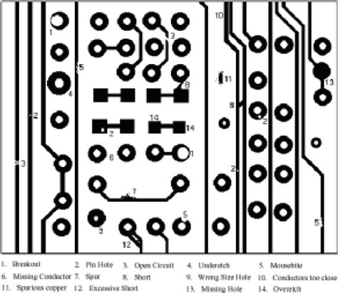
1. Poor Design
One of the primary reasons for PCB Defects is poor design. A poorly designed PCB can lead to various issues such as signal integrity problems, electromagnetic interference (EMI), and thermal management issues. Here are some tips to avoid poor PCB design:
- Use a reliable PCB design software that can detect and prevent design errors.
- Follow the design guidelines and best practices provided by the PCB manufacturer.
- Conduct a thorough design review to ensure that the PCB meets all the requirements and specifications.
- Use appropriate component placement and routing techniques to minimize signal integrity and EMI issues.
2. Incorrect Material Selection
Selecting the wrong material for PCB manufacturing can lead to various defects such as delamination, warping, and poor electrical performance. Here are some tips to avoid incorrect material selection:
- Choose the appropriate PCB substrate material based on the application requirements such as temperature, humidity, and mechanical stress.
- Use high-quality copper foil with the right thickness and surface finish to ensure good electrical conductivity and solderability.
- Select the appropriate solder mask and silkscreen materials that can withstand the manufacturing process and provide good insulation and legibility.

3. Contamination
Contamination is another common reason for PCB defects. Contamination can occur due to various factors such as dust, dirt, oils, and other foreign materials that can affect the PCB’s electrical and mechanical properties. Here are some tips to avoid contamination:
- Maintain a clean and controlled environment during PCB manufacturing.
- Use appropriate cleaning agents and techniques to remove any contaminants from the PCB surface.
- Store the PCBs in a clean and dry environment to prevent contamination during transportation and handling.

4. Inaccurate Drilling
Inaccurate drilling can lead to various PCB defects such as misaligned holes, broken drill bits, and poor electrical connectivity. Here are some tips to avoid inaccurate drilling:
- Use high-quality drill bits with the right diameter and coating to ensure clean and accurate holes.
- Maintain the drill machine regularly to ensure that it is in good working condition.
- Use appropriate drilling parameters such as feed rate, spindle speed, and depth to minimize drill wander and breakage.

5. Overetching or Underetching
Overetching or underetching can occur during the PCB Etching process, leading to various defects such as open circuits, short circuits, and poor signal integrity. Here are some tips to avoid overetching or underetching:
- Use a reliable etching machine with precise control over the etching parameters such as temperature, pressure, and time.
- Monitor the etching process closely to ensure that the PCB is etched to the correct depth and width.
- Use appropriate etchant solutions and concentrations to achieve the desired etching rate and quality.
6. Solder Mask Issues
Solder mask is a protective coating that is applied on the PCB surface to prevent solder bridging and short circuits. However, solder mask issues such as pinholes, blisters, and peeling can occur during the manufacturing process, leading to various defects. Here are some tips to avoid solder mask issues:
- Use high-quality solder mask materials that can withstand the manufacturing process and provide good insulation and adhesion.
- Apply the solder mask evenly and consistently to ensure uniform coverage and thickness.
- Cure the solder mask properly to ensure that it adheres well to the PCB surface and does not peel off.
7. Silkscreen Issues
Silkscreen is used to print text, symbols, and logos on the PCB surface for identification and assembly purposes. However, silkscreen issues such as smudging, fading, and misalignment can occur during the manufacturing process, leading to various defects. Here are some tips to avoid silkscreen issues:
- Use high-quality silkscreen inks that can withstand the manufacturing process and provide good legibility and durability.
- Apply the silkscreen evenly and consistently to ensure uniform coverage and thickness.
- Cure the silkscreen properly to ensure that it adheres well to the PCB surface and does not smudge or fade.
8. Incorrect Component Placement
Incorrect component placement can occur due to various reasons such as human error, machine malfunction, or poor component packaging. This can lead to various defects such as shorts, opens, and poor electrical performance. Here are some tips to avoid incorrect component placement:
- Use a reliable pick-and-place machine with precise control over the placement parameters such as speed, force, and accuracy.
- Verify the component placement using automated optical inspection (AOI) or X-ray inspection to detect any misaligned or missing components.
- Use appropriate component packaging and handling techniques to ensure that the components are not damaged or misplaced during the manufacturing process.
9. Insufficient Solder
Insufficient solder can occur due to various reasons such as poor solder paste printing, inadequate Solder volume, or incorrect reflow parameters. This can lead to various defects such as poor solder joints, open circuits, and reduced reliability. Here are some tips to avoid insufficient solder:
- Use a reliable solder paste printer with precise control over the printing parameters such as pressure, speed, and thickness.
- Apply the appropriate amount of solder paste based on the component size and pad geometry.
- Use appropriate reflow parameters such as temperature, time, and profile to ensure that the solder melts and flows properly.
10. Inadequate Testing
Inadequate testing can lead to various PCB defects going undetected during the manufacturing process, leading to field failures and customer complaints. Here are some tips to avoid inadequate testing:
- Develop a comprehensive testing plan that includes various testing methods such as in-circuit testing (ICT), functional testing, and boundary scan testing.
- Use reliable testing equipment with accurate and repeatable measurements.
- Conduct thorough visual inspection and X-ray inspection to detect any visible defects or anomalies.
| Defect | Cause | Solution |
|---|---|---|
| Poor Design | Incorrect design rules, signal integrity issues, EMI problems | Use reliable PCB design software, follow best practices, conduct design review |
| Incorrect Material Selection | Wrong substrate, copper foil, solder mask, or silkscreen materials | Choose appropriate materials based on application requirements |
| Contamination | Dust, dirt, oils, and other foreign materials | Maintain clean environment, use proper cleaning agents and techniques |
| Inaccurate Drilling | Misaligned holes, broken drill bits, poor electrical connectivity | Use high-quality drill bits, maintain drill machine, use appropriate parameters |
| Overetching/Underetching | Open circuits, short circuits, poor signal integrity | Use reliable etching machine, monitor etching process, use appropriate etchant |
| Solder Mask Issues | Pinholes, blisters, peeling | Use high-quality materials, apply evenly, cure properly |
| Silkscreen Issues | Smudging, fading, misalignment | Use high-quality inks, apply evenly, cure properly |
| Incorrect Component Placement | Shorts, opens, poor electrical performance | Use reliable pick-and-place machine, verify placement, use proper packaging |
| Insufficient Solder | Poor solder joints, open circuits, reduced reliability | Use reliable solder paste printer, apply appropriate amount, use proper reflow |
| Inadequate Testing | Undetected defects, field failures, customer complaints | Develop comprehensive testing plan, use reliable equipment, conduct thorough inspection |
Frequently Asked Questions (FAQ)
1. What are the most common PCB manufacturing defects?
The most common PCB manufacturing defects include poor design, incorrect material selection, contamination, inaccurate drilling, overetching/underetching, solder mask issues, silkscreen issues, incorrect component placement, insufficient solder, and inadequate testing.
2. How can I prevent PCB design errors?
To prevent PCB design errors, use a reliable PCB design software that can detect and prevent design errors, follow the design guidelines and best practices provided by the PCB manufacturer, conduct a thorough design review, and use appropriate component placement and routing techniques.
3. What are the consequences of using the wrong materials for PCB manufacturing?
Using the wrong materials for PCB manufacturing can lead to various defects such as delamination, warping, and poor electrical performance. It is important to choose the appropriate PCB substrate material, copper foil, solder mask, and silkscreen materials based on the application requirements.
4. How can I ensure accurate component placement during PCB Assembly?
To ensure accurate component placement during PCB assembly, use a reliable pick-and-place machine with precise control over the placement parameters, verify the component placement using automated optical inspection (AOI) or X-ray inspection, and use appropriate component packaging and handling techniques.
5. What are the benefits of conducting thorough PCB Testing?
Conducting thorough PCB testing can help detect various defects and anomalies that may go undetected during the manufacturing process, leading to field failures and customer complaints. It is important to develop a comprehensive testing plan that includes various testing methods such as in-circuit testing (ICT), functional testing, and boundary scan testing, and use reliable testing equipment with accurate and repeatable measurements.


Leave a Reply