Introduction to PCB Quality
Printed Circuit Boards (PCBs) are the backbone of modern electronics. They are used in almost every electronic device, from smartphones and computers to medical equipment and aerospace systems. The quality of a PCB can make or break the functionality, reliability, and longevity of the device it powers. Therefore, it is crucial to understand what PCB quality entails and how to ensure that your PCBs meet the highest standards.
In this comprehensive article, we will dive deep into the world of PCB quality. We will explore the various factors that contribute to PCB quality, the standards and certifications that govern PCB manufacturing, and the best practices for designing, fabricating, and testing high-quality PCBs. Whether you are an electronics engineer, a PCB designer, or a curious tech enthusiast, this article will provide you with everything you need to know about PCB quality.
What is PCB Quality?
PCB quality refers to the overall performance, reliability, and durability of a printed circuit board. A high-quality PCB is one that meets or exceeds the specified requirements and functions as intended throughout its expected lifetime. PCB quality is determined by a combination of factors, including:
- Material selection
- Design and layout
- Manufacturing processes
- Quality control and testing
- Packaging and shipping
Each of these factors plays a crucial role in ensuring that the final PCB product is of the highest quality. Let’s take a closer look at each of these factors.
Material Selection
The choice of materials used in PCB fabrication can significantly impact the quality of the final product. The most common materials used in PCB manufacturing are:
- Substrate materials: FR-4, Rogers, Polyimide, Aluminum, etc.
- Copper foil: Electrodeposited (ED) or Rolled Annealed (RA)
- Solder mask: Liquid photoimageable (LPI), Dry film, or Ink
- Silkscreen: Epoxy, UV curable, or Ink
The selection of these materials depends on the specific requirements of the PCB, such as the intended application, operating environment, and budget. For example, FR-4 is the most commonly used substrate material due to its excellent electrical and mechanical properties, as well as its cost-effectiveness. However, for high-frequency or high-speed applications, materials like Rogers or Polyimide may be more suitable.
Design and Layout
The design and layout of a PCB can have a significant impact on its quality and performance. A well-designed PCB should follow the industry standards and best practices, such as:
- Proper component placement and orientation
- Adequate spacing between traces and components
- Proper grounding and shielding
- Minimizing crosstalk and electromagnetic interference (EMI)
- Ensuring manufacturability and testability
PCB designers use specialized software tools, such as Altium Designer, Eagle, or KiCad, to create the schematic and layout files for the PCB. These files are then sent to the PCB manufacturer for fabrication.
Manufacturing Processes
The manufacturing process is where the actual PCB is fabricated based on the design files. The quality of the PCB largely depends on the precision and consistency of the manufacturing processes. The key steps in PCB manufacturing include:
- Copper etching and plating
- Drilling and routing
- Solder mask application
- Silkscreen printing
- Surface finish application (HASL, ENIG, OSP, etc.)
Each of these steps must be performed with utmost care and attention to detail to ensure that the final PCB meets the specified requirements. PCB manufacturers use specialized equipment and processes, such as photolithography, chemical etching, and automated optical inspection (AOI), to achieve high precision and consistency.
Quality Control and Testing
Quality control and testing are critical steps in ensuring the quality of the final PCB product. PCB manufacturers employ various quality control measures throughout the manufacturing process, such as:
- Incoming material inspection
- In-process inspection and testing
- Final inspection and testing
These measures help identify and correct any defects or deviations from the specified requirements before the PCB is shipped to the customer. Some common testing methods used in PCB manufacturing include:
- Visual inspection
- Automated optical inspection (AOI)
- X-ray inspection
- Electrical testing (continuity, isolation, etc.)
- Functional testing
- Environmental testing (temperature, humidity, vibration, etc.)
Packaging and Shipping
The final step in ensuring PCB quality is proper packaging and shipping. PCBs are delicate components that can be easily damaged during transportation. Therefore, PCB manufacturers use specialized packaging materials and techniques to protect the PCBs from physical damage, moisture, and electrostatic discharge (ESD). Some common packaging methods include:
- Vacuum packaging
- ESD shielding bags
- Bubble wrap or foam padding
- Rigid boxes or containers
Proper labeling and documentation, such as packing slips and certificates of conformance (CoC), are also important for traceability and quality assurance.

PCB Quality Standards and Certifications
To ensure consistent and reliable PCB quality, various industry standards and certifications have been established. These standards provide guidelines and requirements for PCB design, manufacturing, and testing. Some of the most widely recognized PCB quality standards include:
IPC Standards
IPC (formerly known as the Institute for Printed Circuits) is a global trade association that develops and publishes standards for the electronics industry. Some of the key IPC standards related to PCB quality include:
- IPC-A-600: Acceptability of Printed Boards
- IPC-6012: Qualification and Performance Specification for Rigid Printed Boards
- IPC-6013: Qualification and Performance Specification for Flexible Printed Boards
- IPC-A-610: Acceptability of Electronic Assemblies
These standards provide detailed requirements and acceptance criteria for various aspects of PCB quality, such as copper thickness, hole size, solder mask coverage, and surface finish quality.
ISO Standards
ISO (International Organization for Standardization) is an international standard-setting body that develops and publishes standards for various industries. Some of the key ISO standards related to PCB quality include:
- ISO 9001: Quality Management Systems
- ISO 14001: Environmental Management Systems
- ISO/TS 16949: Quality Management Systems for Automotive Production
These standards provide guidelines for establishing and maintaining quality management systems, environmental management systems, and other organizational processes that impact PCB quality.
UL Standards
UL (Underwriters Laboratories) is a global safety certification company that develops and publishes standards for product safety. Some of the key UL standards related to PCB quality include:
- UL 94: Standard for Safety of Flammability of Plastic Materials
- UL 746A: Standard for Polymeric Materials – Short Term Property Evaluations
- UL 796: Standard for Printed-Wiring Boards
These standards provide requirements for the flammability, thermal stability, and other safety-related properties of PCB materials and components.
PCB manufacturers can obtain certifications from these organizations by demonstrating compliance with the relevant standards through audits and inspections. Customers can look for these certifications as a mark of quality assurance when selecting a PCB manufacturer.

Best Practices for High-Quality PCB Design and Manufacturing
To ensure the highest quality of your PCBs, it is important to follow best practices throughout the design and manufacturing process. Here are some key best practices to keep in mind:
Design Best Practices
- Use a reputable PCB design software and follow the software’s design rules and guidelines
- Follow the IPC design standards and recommendations
- Use a consistent and clear naming convention for components, nets, and layers
- Use appropriate trace widths and spacing based on the signal requirements and manufacturability
- Use appropriate via sizes and placement based on the manufacturability and reliability
- Use appropriate component footprints and land patterns based on the manufacturer’s recommendations
- Use appropriate silkscreen and assembly information for easy identification and assembly
- Use appropriate design for manufacturing (DFM) and design for testing (DFT) techniques to ensure manufacturability and testability
Manufacturing Best Practices
- Use a reputable PCB manufacturer with proven track record and certifications
- Provide clear and complete manufacturing files, including Gerber files, drill files, and assembly files
- Communicate clearly with the manufacturer about the project requirements, timeline, and budget
- Request a design for manufacturability (DFM) review before placing the order
- Request a first article inspection (FAI) or pre-production sample before mass production
- Verify the quality of the received PCBs through visual inspection, electrical testing, and functional testing
- Provide feedback to the manufacturer about any quality issues or concerns
By following these best practices, you can minimize the risk of quality issues and ensure that your PCBs meet the highest standards of performance and reliability.

Common PCB Quality Issues and How to Avoid Them
Despite the best efforts of PCB designers and manufacturers, quality issues can still arise. Here are some of the most common PCB quality issues and how to avoid them:
Copper Thickness Variations
Copper thickness variations can occur due to uneven plating or etching during the manufacturing process. This can lead to inconsistent electrical performance and reliability issues. To avoid this issue:
- Use a reputable PCB manufacturer with tight process controls
- Specify the copper thickness requirements clearly in the manufacturing files
- Request a copper thickness report or measurement data from the manufacturer
Solder Mask Defects
Solder mask defects, such as pinholes, blisters, or peeling, can expose the underlying copper and lead to short circuits or corrosion. To avoid this issue:
- Use a high-quality solder mask material and process
- Follow the IPC solder mask standards and requirements
- Perform a visual inspection of the solder mask coverage and adhesion
Drill and Routing Errors
Drill and routing errors, such as misaligned or oversized holes, can lead to assembly and reliability issues. To avoid this issue:
- Use a reputable PCB manufacturer with precision drilling and routing equipment
- Specify the drill and routing requirements clearly in the manufacturing files
- Perform a visual inspection of the drilled and routed features
Silkscreen Legibility
Poor silkscreen legibility can make it difficult to identify components and assembly information. To avoid this issue:
- Use a high-quality silkscreen ink and process
- Follow the IPC silkscreen standards and requirements
- Perform a visual inspection of the silkscreen legibility and alignment
Bow and Twist
Excessive bow and twist can make the PCB difficult to assemble and can cause reliability issues. To avoid this issue:
- Use a high-quality substrate material with low moisture absorption
- Follow the IPC bow and twist standards and requirements
- Perform a visual inspection of the PCB flatness and measure the bow and twist if necessary
By being aware of these common quality issues and taking steps to avoid them, you can ensure that your PCBs meet the highest standards of quality and reliability.
PCB Quality Testing Methods
To verify the quality of PCBs, various testing methods are used throughout the manufacturing process and after the PCBs are fabricated. Here are some of the most common PCB quality testing methods:
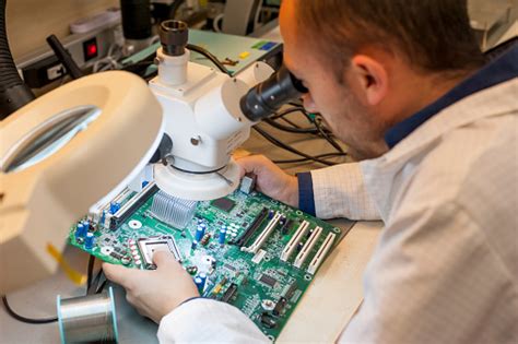
Visual Inspection
Visual inspection is the most basic and widely used method of PCB quality testing. It involves visually examining the PCB for any defects or anomalies, such as:
- Copper thickness variations
- Solder mask defects
- Drill and routing errors
- Silkscreen legibility
- Bow and twist
Visual inspection can be performed manually by trained operators or automatically using automated optical inspection (AOI) equipment.
Automated Optical Inspection (AOI)
AOI is a computer-based system that uses high-resolution cameras and image processing software to automatically inspect PCBs for defects. AOI can detect a wide range of defects, such as:
- Solder bridging or opens
- Component placement errors
- Solder paste defects
- Copper pattern defects
AOI is faster and more consistent than manual visual inspection and can detect defects that may be missed by the human eye.
X-Ray Inspection
X-ray inspection is used to detect defects that are not visible on the surface of the PCB, such as:
- Voids or cracks in solder joints
- Broken or missing wire bonds
- Delamination or voids in the substrate
X-ray inspection uses high-energy X-rays to create a detailed image of the internal structure of the PCB. This allows defects to be detected and analyzed without destroying the PCB.
Electrical Testing
Electrical testing is used to verify the electrical performance and functionality of the PCB. There are several types of electrical testing, including:
- Continuity testing: Verifies that all the connections on the PCB are intact and have the correct resistance
- Isolation testing: Verifies that there are no short circuits or leakage paths between different parts of the PCB
- Functional testing: Verifies that the PCB performs its intended function under various operating conditions
Electrical testing can be performed using specialized test equipment, such as flying probe testers, in-circuit testers, or functional test systems.
Environmental Testing
Environmental testing is used to verify the reliability and durability of the PCB under various environmental conditions, such as:
- Temperature cycling: Exposes the PCB to repeated cycles of high and low temperatures to simulate thermal stress
- Humidity testing: Exposes the PCB to high humidity levels to simulate moisture exposure
- Vibration testing: Exposes the PCB to mechanical vibrations to simulate transportation and handling stress
Environmental testing can help identify potential reliability issues and ensure that the PCB can withstand the intended operating environment.
By using a combination of these testing methods, PCB manufacturers can ensure that the PCBs meet the specified quality requirements and are free from defects that could impact their performance or reliability.
Conclusion
PCB quality is a critical factor in the success of any electronic product. By understanding the various factors that contribute to PCB quality, following industry standards and best practices, and using appropriate testing methods, you can ensure that your PCBs meet the highest standards of performance, reliability, and durability.
Whether you are a PCB designer, manufacturer, or end-user, investing in PCB quality is essential for the long-term success of your products and business. By partnering with reputable PCB manufacturers and suppliers, staying up-to-date with the latest industry trends and technologies, and continuously improving your processes and practices, you can achieve the highest levels of PCB quality and customer satisfaction.
FAQ
- What is the difference between PCB quality and PCB reliability?
-
PCB quality refers to the conformance of the PCB to the specified requirements and standards, while PCB reliability refers to the ability of the PCB to perform its intended function over its expected lifetime under specified operating conditions.
-
What are the most common PCB quality standards?
-
The most common PCB quality standards are IPC standards, such as IPC-A-600 for acceptability of printed boards, IPC-6012 for qualification and performance of rigid PCBs, and IPC-A-610 for acceptability of electronic assemblies.
-
How can I ensure the quality of my PCBs?
-
To ensure the quality of your PCBs, you should follow industry standards and best practices for PCB design and manufacturing, use reputable PCB manufacturers and suppliers, and perform appropriate quality testing and inspection throughout the manufacturing process.
-
What are the most common PCB quality issues?
-
The most common PCB quality issues include copper thickness variations, solder mask defects, drill and routing errors, silkscreen legibility issues, and excessive bow and twist.
-
What are the benefits of investing in PCB quality?
- The benefits of investing in PCB quality include improved product performance and reliability, reduced warranty and repair costs, increased customer satisfaction and loyalty, and enhanced brand reputation and market competitiveness.


Leave a Reply