Introduction to Fast Print PCB
Fast Print PCB is a quick and efficient way to produce printed circuit boards (PCBs) for electronic projects. By utilizing advanced manufacturing techniques and streamlined processes, FastPrintPCB enables designers and engineers to rapidly prototype and iterate on their designs, significantly reducing the time and cost associated with traditional PCB fabrication methods.
In this article, we will explore the key factors that contribute to creating the perfect Fast Print PCB, ensuring high-quality results and reliable performance for your electronic projects.
The Importance of PCB Design in Fast Print PCB
Designing for Manufacturability
When designing a PCB for Fast Print PCB, it is crucial to consider the manufacturability of your design. This means adhering to the design rules and guidelines set forth by the FastPrintPCB service provider, such as minimum trace widths, clearances, and hole sizes. By designing with manufacturability in mind, you can ensure that your PCB will be produced accurately and efficiently, minimizing the risk of errors and delays.
Optimizing Component Placement
Proper component placement is essential for creating a perfect Fast Print PCB. When placing components on your board, consider factors such as signal integrity, thermal management, and mechanical constraints. Strategically positioning components can help minimize signal interference, reduce the risk of thermal issues, and improve the overall reliability of your PCB.
Utilizing Design Software and Tools
To streamline the PCB design process for Fast Print PCB, it is recommended to use specialized PCB design software and tools. These tools often include features such as automated design rule checking (DRC), which helps identify and resolve potential design issues before submitting your files for fabrication. Additionally, many FastPrintPCB service providers offer their own design templates and guidelines, which can be easily integrated into popular PCB design software packages.

Material Selection for Fast Print PCB
Choosing the Right Substrate Material
The choice of substrate material is a critical factor in creating the perfect Fast Print PCB. The most commonly used substrate materials for FastPrintPCB include FR-4, a glass-reinforced epoxy laminate, and polyimide, a high-temperature resistant polymer. When selecting a substrate material, consider the electrical, thermal, and mechanical requirements of your application, as well as the cost and availability of the material.
Understanding Copper Weights and Thicknesses
Copper weight and thickness play a significant role in the performance and manufacturability of your Fast Print PCB. Copper weight refers to the amount of copper deposited on the substrate, typically measured in ounces per square foot (oz/ft²). Thicker copper layers can carry more current and provide better thermal dissipation, but may also increase the cost and complexity of manufacturing. When choosing a copper weight for your FastPrintPCB, strike a balance between performance requirements and manufacturing feasibility.
Specifying Surface Finishes
The surface finish of your Fast Print PCB serves both functional and aesthetic purposes. Common surface finishes for FastPrintPCB include Hot Air Solder Leveling (HASL), Immersion Silver (IAg), and Electroless Nickel Immersion Gold (ENIG). Each surface finish has its own advantages and disadvantages in terms of cost, durability, and solderability. Select a surface finish that best suits your application’s requirements and budget.

Manufacturing Process Considerations
Understanding the FastPrintPCB Fabrication Process
To create the perfect Fast Print PCB, it is important to understand the basic steps involved in the fabrication process. The FastPrintPCB manufacturing process typically includes the following stages:
- Pre-production: Design files are checked and prepared for fabrication.
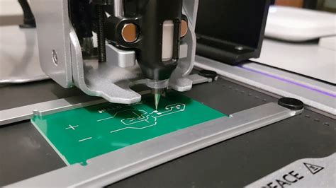
- Printing: The PCB design is printed onto the substrate material using advanced printing techniques.
- Etching: Unwanted copper is removed from the substrate, leaving only the desired traces and pads.
- Drilling: Holes are drilled into the PCB for component mounting and interconnections.
- Surface Finishing: The selected surface finish is applied to the PCB.
- Solder Mask Application: A protective solder mask is applied to the PCB to insulate and protect the traces.
- Silkscreen Printing: Component labels and other markings are printed onto the PCB using silkscreen printing.
- Electrical Testing: The PCB undergoes electrical testing to ensure proper functionality.
- Final Inspection: The PCB is visually inspected for any defects or issues before packaging and shipping.
Choosing the Right Board Thickness
Board thickness is another important factor to consider when creating a Fast Print PCB. The most common board thicknesses for FastPrintPCB range from 0.6mm to 2.0mm. Thinner boards are generally more cost-effective and easier to manufacture, while thicker boards offer better mechanical stability and thermal performance. Choose a board thickness that balances your application’s requirements with manufacturing feasibility and cost.
Specifying Layer Stackups
For multi-layer Fast Print PCBs, specifying the proper layer stackup is crucial for ensuring signal integrity and manufacturability. A layer stackup defines the arrangement of copper layers, insulating layers, and laminate materials within the PCB. When designing your layer stackup, consider factors such as signal routing, impedance control, and manufacturability constraints. Consult with your FastPrintPCB service provider to determine the optimal layer stackup for your design.

Quality Control and Testing
Implementing Design for Testing (DFT)
To ensure the perfect Fast Print PCB, it is essential to implement Design for Testing (DFT) principles during the design phase. DFT involves incorporating testability features into your PCB design, such as test points, boundary scan architecture, and built-in self-test (BIST) circuitry. By designing for testability, you can facilitate efficient and comprehensive testing of your PCB, reducing the risk of defects and improving overall quality.
Leveraging Automated Optical Inspection (AOI)
Automated Optical Inspection (AOI) is a powerful tool for ensuring the quality of your Fast Print PCB. AOI systems use high-resolution cameras and advanced image processing algorithms to detect and identify manufacturing defects, such as missing components, solder bridges, and incorrect component placement. By leveraging AOI technology, FastPrintPCB service providers can quickly and accurately inspect PCBs, ensuring that only high-quality boards are delivered to customers.
Conducting Functional Testing
In addition to AOI, functional testing is a critical step in creating the perfect Fast Print PCB. Functional testing involves verifying that the PCB performs as intended under real-world operating conditions. This may include testing the board’s electrical characteristics, signal integrity, and thermal performance. By conducting thorough functional testing, you can identify and address any issues before the PCB is put into production, ensuring reliable performance in the final application.
FastPrintPCB Service Provider Selection
Evaluating Turnaround Time and Cost
When selecting a FastPrintPCB service provider, it is important to evaluate their turnaround time and cost. Fast turnaround times are essential for rapid prototyping and iterative design, while competitive pricing can help keep your project within budget. Look for a service provider that offers a balance of speed and affordability, without compromising on quality.
Assessing Quality and Reliability
The quality and reliability of your Fast Print PCB are paramount to the success of your electronic project. When choosing a FastPrintPCB service provider, assess their reputation for delivering high-quality PCBs consistently. Look for customer reviews, case studies, and testimonials that speak to the provider’s commitment to quality and reliability. Additionally, inquire about their quality control processes and certifications, such as ISO 9001 or UL listing.
Considering Customer Support and Technical Expertise
Creating the perfect Fast Print PCB often requires close collaboration between the designer and the service provider. When selecting a FastPrintPCB partner, consider their level of customer support and technical expertise. Look for a provider that offers responsive and knowledgeable support staff, as well as resources such as design guides, tutorials, and FAQs. A service provider with strong technical expertise can also provide valuable guidance and recommendations throughout the design and manufacturing process, helping you optimize your PCB for the best possible results.
Frequently Asked Questions (FAQ)
1. What is the minimum feature size for Fast Print PCB?
The minimum feature size for Fast Print PCB varies depending on the service provider and the specific manufacturing process used. Typically, FastPrintPCB services can accommodate minimum trace widths and spacings down to 3-4 mils (0.076-0.102mm) and minimum hole sizes of 8-10 mils (0.203-0.254mm). However, it is always best to consult with your chosen service provider for their specific capabilities and design guidelines.
2. How long does it take to receive a Fast Print PCB Prototype?
Turnaround times for Fast Print PCB Prototypes vary depending on the service provider, the complexity of the design, and the chosen manufacturing options. Many FastPrintPCB services offer standard turnaround times of 24-72 hours for simple designs, while more complex boards may take 5-7 business days. Some providers also offer expedited manufacturing options for even faster turnaround times, although these may come at a higher cost.
3. Can I specify custom soldermask and silkscreen colors for my Fast Print PCB?
Yes, most FastPrintPCB service providers offer the option to specify custom soldermask and silkscreen colors for your PCB. Common soldermask color options include green, red, blue, yellow, and black, while silkscreen colors typically include white, black, and yellow. Some providers may also offer additional color options or even custom color matching for a fee. Be sure to check with your chosen service provider for their available color options and any associated costs.
4. What file formats are required for submitting Fast Print PCB designs?
FastPrintPCB service providers typically require design files to be submitted in industry-standard formats, such as Gerber files (RS-274X) and drill files (Excellon). Most PCB design software packages can generate these file formats as part of the output process. Some service providers may also accept additional file formats, such as ODB++ or IPC-2581, for more comprehensive design data exchange. It is important to check with your chosen provider for their specific file format requirements and any necessary export settings.
5. How can I ensure the best possible quality for my Fast Print PCB?
To ensure the best possible quality for your Fast Print PCB, consider the following tips:
- Follow the design guidelines and rules provided by your chosen FastPrintPCB service provider.
- Use reputable PCB design software and tools, and perform thorough design rule checks (DRC) before submitting your files.
- Choose high-quality materials and finishes that are appropriate for your application’s requirements.
- Implement Design for Testing (DFT) principles to facilitate efficient and comprehensive testing.
- Select a FastPrintPCB service provider with a strong reputation for quality, reliability, and customer support.
- Communicate clearly with your service provider throughout the design and manufacturing process, and be open to their feedback and recommendations.
By following these guidelines and working closely with a trusted FastPrintPCB partner, you can ensure that your Fast Print PCB meets the highest standards of quality and performance.
Conclusion
Creating the perfect Fast Print PCB requires careful consideration of design, materials, manufacturing processes, quality control, and service provider selection. By understanding the key factors that contribute to FastPrintPCB success, designers and engineers can optimize their designs for manufacturability, reliability, and performance.
From choosing the right substrate materials and specifying appropriate layer stackups to implementing DFT principles and leveraging automated inspection technologies, each step of the Fast Print PCB process plays a critical role in achieving the best possible results.
Ultimately, the success of your Fast Print PCB project depends on close collaboration with a trusted and experienced FastPrintPCB service provider. By partnering with a provider that offers a combination of technical expertise, high-quality manufacturing, and responsive customer support, you can bring your electronic designs to life quickly, efficiently, and with the highest level of quality.
As the demand for rapid prototyping and agile product development continues to grow, Fast Print PCB technology will undoubtedly play an increasingly important role in the electronics industry. By staying informed about the latest advancements and best practices in FastPrintPCB design and manufacturing, designers and engineers can unlock new possibilities for innovation and success in their electronic projects.


Leave a Reply