Understanding the Need for Power Supply Bypassing
Power supply bypassing is the practice of adding capacitors in parallel with power supply rails to provide a low-impedance path for high-frequency noise and transient currents. The main objectives of bypassing are:
- Reducing voltage fluctuations caused by sudden changes in current demand
- Filtering out high-frequency noise generated by digital circuits
- Providing a local energy reserve for fast-switching components
- Improving overall power supply stability and signal integrity
Without proper bypassing, PCBs can suffer from various issues, such as:
- Power supply ripple and noise
- Ground bounce and voltage spikes
- Electromagnetic interference (EMI)
- Signal distortion and crosstalk
- Reduced component lifespan and reliability
Key Components for Power Supply Bypassing
The primary components used for power supply bypassing are capacitors. There are several types of capacitors commonly used for this purpose:
Ceramic Capacitors
Ceramic capacitors are the most widely used type for power supply bypassing due to their low equivalent series resistance (ESR), low inductance, and wide range of available values. They are effective at high frequencies and can be placed close to the power pins of ICs.
Tantalum Capacitors
Tantalum capacitors offer high capacitance values in a small package size. They have lower ESR compared to electrolytic capacitors but higher than ceramic capacitors. Tantalum capacitors are often used for bulk decoupling and low-frequency bypassing.
Electrolytic Capacitors
Electrolytic capacitors provide the highest capacitance values but have higher ESR and lower frequency response compared to ceramic and tantalum capacitors. They are commonly used for bulk decoupling and filtering at the power supply input.
The table below summarizes the characteristics of these capacitor types:
| Capacitor Type | ESR | Inductance | Frequency Response | Typical Values |
|---|---|---|---|---|
| Ceramic | Low | Low | High | pF to μF |
| Tantalum | Medium | Medium | Medium | μF to hundreds of μF |
| Electrolytic | High | High | Low | μF to thousands of μF |

Bypassing Techniques and Best Practices
Decoupling Capacitor Placement
Proper placement of decoupling capacitors is crucial for effective bypassing. The general guidelines are:
- Place decoupling capacitors as close as possible to the power pins of ICs
- Minimize the trace length between the capacitor and the IC power pin
- Use multiple capacitors in parallel to reduce the effective inductance
- Place low-value ceramic capacitors closest to the IC, followed by higher-value capacitors
- Avoid placing capacitors on the opposite side of the PCB from the IC
Decoupling Capacitor Selection
Selecting the right decoupling capacitors involves considering several factors:
- Capacitance value: Choose values based on the frequency range and current requirements of the circuit
- Voltage rating: Ensure the capacitor’s voltage rating exceeds the maximum expected voltage, with a safety margin
- ESR: Lower ESR is generally preferred for better high-frequency performance
- Temperature stability: Consider the capacitor’s temperature coefficient and operating temperature range
- Package size: Select package sizes that fit the available PCB space and layout constraints
Power and Ground Plane Design
Proper design of power and ground planes is essential for effective bypassing and minimizing impedance:
- Use dedicated power and ground planes on separate layers
- Provide adequate copper pour for low-impedance power distribution
- Minimize the distance between power and ground planes to reduce inductance
- Use multiple vias to connect decoupling capacitors to power and ground planes
- Avoid splitting power and ground planes, as it can create high-impedance paths
Bulk Decoupling
In addition to local decoupling at ICs, bulk decoupling is used to provide a low-impedance path for low-frequency currents and to filter noise from the power supply:
- Place bulk decoupling capacitors near the power supply input
- Use electrolytic or tantalum capacitors with high capacitance values (e.g., 10 μF to 1000 μF)
- Parallel multiple capacitors to reduce the effective ESR and increase the total capacitance
- Consider using ferrite beads or inductors in series with the power supply input for additional filtering
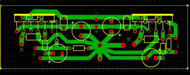
 RAYMING-PCB-manufacturing-and-asssembly.jpg” alt=”” class=”wp-image-136″ srcset=”” sizes=”(max-width: 1024px) 100vw, 1024px”>
PCB Layout Considerations for Power Supply Bypassing
Proper PCB layout is crucial for effective power supply bypassing. Here are some key considerations:
Component Placement
- Group components with similar power requirements together
- Place decoupling capacitors close to the power pins of ICs
- Orient capacitors to minimize the loop area between the capacitor and the IC
- Avoid placing components or traces between the decoupling capacitor and the IC
Trace Routing
- Route power and ground traces as short and wide as possible
- Use solid power and ground planes instead of thin traces
- Avoid routing high-speed signals near power traces to minimize crosstalk
- Use via stitching to connect power and ground planes on different layers
Via Placement
- Place vias close to the power pins of ICs for low-impedance connections
- Use multiple vias in parallel to reduce the effective inductance
- Avoid sharing vias between different power domains or signal traces
- Consider using blind or Buried Vias for dense PCB layouts
Ground Plane Stitching
- Use a sufficient number of vias to stitch ground planes together
- Place ground stitching vias near the edges of the PCB and under connectors
- Avoid placing ground stitching vias too close to sensitive analog circuits
- Use a grid pattern for even distribution of ground stitching vias

Measuring and Verifying Power Supply Bypassing
To ensure effective power supply bypassing, it is important to measure and verify the performance of the bypassing network. Some common techniques include:
Time-Domain Measurements
- Use an oscilloscope to measure voltage ripple and noise on the power supply rails
- Measure the transient response of the power supply to sudden load changes
- Verify that the voltage remains within the specified tolerance during transients
Frequency-Domain Measurements
- Use a spectrum analyzer or network analyzer to measure the impedance of the power distribution network
- Verify that the impedance remains low over the frequency range of interest
- Check for resonances or peaks in the impedance profile that could indicate inadequate bypassing
Simulation and Modeling
- Use simulation tools to model the power distribution network and predict its performance
- Analyze the impact of component placement, trace routing, and via placement on bypassing effectiveness
- Optimize the bypassing network based on simulation results before finalizing the PCB layout
FAQ
1. What is the purpose of power supply bypassing?
Power supply bypassing is used to reduce voltage fluctuations, filter out high-frequency noise, provide a local energy reserve for fast-switching components, and improve overall power supply stability and signal integrity on PCBs.
2. What types of capacitors are commonly used for power supply bypassing?
The most common types of capacitors used for power supply bypassing are ceramic capacitors, tantalum capacitors, and electrolytic capacitors. Ceramic capacitors are widely used for high-frequency bypassing, while tantalum and electrolytic capacitors are used for bulk decoupling and low-frequency filtering.
3. How close should decoupling capacitors be placed to ICs?
Decoupling capacitors should be placed as close as possible to the power pins of ICs to minimize the trace inductance and provide effective high-frequency bypassing. The general guideline is to place the capacitors within a few millimeters of the IC power pins.
4. What is the difference between local decoupling and bulk decoupling?
Local decoupling refers to the placement of capacitors close to the power pins of individual ICs to provide a low-impedance path for high-frequency noise and transient currents. Bulk decoupling, on the other hand, involves placing larger capacitors near the power supply input to filter low-frequency noise and provide a low-impedance path for low-frequency currents.
5. How can I verify the effectiveness of my power supply bypassing?
To verify the effectiveness of power supply bypassing, you can use time-domain measurements with an oscilloscope to observe voltage ripple and transient response, frequency-domain measurements with a spectrum analyzer or network analyzer to measure the impedance of the power distribution network, and simulation tools to model and optimize the bypassing network before finalizing the PCB layout.
Conclusion
Proper power supply bypassing is essential for ensuring the stable operation and high performance of PCBs. By understanding the principles, techniques, and best practices for effective bypassing, designers can mitigate power supply issues, reduce noise and interference, and improve overall system reliability.
Key points to remember include:
- Choosing the right capacitors based on capacitance value, voltage rating, ESR, temperature stability, and package size
- Placing decoupling capacitors close to the power pins of ICs and minimizing trace inductance
- Designing dedicated power and ground planes with adequate copper pour and minimized impedance
- Considering bulk decoupling near the power supply input for low-frequency filtering
- Optimizing PCB layout for component placement, trace routing, via placement, and ground plane stitching
- Measuring and verifying the performance of the bypassing network using time-domain, frequency-domain, and simulation techniques
By following these guidelines and continuously refining your power supply bypassing strategies, you can design PCBs that deliver robust, reliable, and high-performance operation in a wide range of applications.


Leave a Reply