Introduction to PCB Current Calculators
A printed circuit board (PCB) current calculator is an essential tool for electrical engineers and PCB designers. It allows you to accurately determine the current carrying capacity of the traces on a PCB based on factors such as the trace width, thickness, temperature rise, and ambient temperature.
Using a PCB current calculator ensures that your PCB traces are sized appropriately to handle the required current without overheating or failing prematurely. This is critical for the reliability and longevity of the PCB and the overall electronic device.
In this comprehensive article, we will dive deep into the world of PCB current calculators. We’ll cover the basic concepts, the key factors that influence current capacity, how to use a PCB current calculator, and best practices for PCB trace current design. Whether you’re a seasoned electrical engineer or just starting out, this guide will provide you with the knowledge you need to effectively use a PCB current calculator in your designs.
How Does a PCB Current Calculator Work?
The Basics of PCB Trace Current Capacity
To understand how a PCB current calculator works, we first need to grasp the fundamentals of PCB trace current capacity. The current carrying capacity of a PCB trace depends on several factors:
- Trace width: Wider traces can carry more current than narrower traces.
- Trace thickness: Thicker traces have higher current capacity compared to thinner traces.
- Temperature rise: The acceptable temperature rise of the trace limits the current it can carry without overheating.
- Ambient temperature: Higher ambient temperatures reduce the current carrying capacity of the trace.
The relationship between these factors is governed by the following equation:
I = k * ΔT^0.44 * A^0.725
Where:
– I is the maximum current in amps
– ΔT is the allowed temperature rise above ambient in °C
– A is the cross-sectional area of the trace in mils² (1 mil = 0.001 inch)
– k is a constant that depends on the trace material (for copper, k = 0.048)
Calculating the Cross-Sectional Area
To use the current capacity equation, we need to calculate the cross-sectional area of the trace. The cross-sectional area is the product of the trace width and thickness:
A = width (mils) * thickness (mils)
For example, if a trace is 10 mils wide and 1.4 mils thick (1 oz copper), its cross-sectional area is:
A = 10 mils * 1.4 mils = 14 mils²
Determining the Acceptable Temperature Rise
The acceptable temperature rise depends on several factors, such as the PCB material, the component ratings, and the operating environment. As a general rule, a temperature rise of 10°C to 20°C is considered safe for most applications.
However, in high-reliability or harsh environment applications, a lower temperature rise may be necessary. It’s essential to consult the PCB material datasheet and component specifications to determine the appropriate temperature rise limit.
Using a PCB Current Calculator
Now that we understand the basics, let’s see how to use a PCB current calculator. Most PCB current calculators will ask for the following inputs:
- Trace width (in mils or mm)
- Trace thickness (in mils, mm, or copper weight)
- Acceptable temperature rise (in °C)
- Ambient temperature (in °C)
Once you enter these values, the calculator will output the maximum current capacity of the trace. Here’s an example:
| Input | Value |
|---|---|
| Trace width | 10 mils |
| Trace thickness | 1.4 mils |
| Acceptable temp. rise | 15°C |
| Ambient temperature | 25°C |
For these inputs, a typical PCB current calculator might output a maximum current capacity of approximately 1.0A.
It’s important to note that PCB current calculators provide a theoretical maximum based on the given inputs. In practice, it’s recommended to derate the maximum current by a factor of 20% to 50% to account for variations in manufacturing, material properties, and operating conditions.
Factors Affecting PCB Trace Current Capacity
Trace Geometry
The width and thickness of a PCB trace directly impact its current carrying capacity. Wider and thicker traces have lower resistance and can handle higher currents without excessive heating.
However, increasing trace width and thickness comes with trade-offs. Wider traces consume more board space, which can make routing more challenging and increase the overall PCB size. Thicker traces require more copper, which adds to the PCB cost and weight.
As a PCB designer, it’s essential to find the right balance between current capacity, routing efficiency, and cost. This is where a PCB current calculator becomes invaluable, as it allows you to quickly experiment with different trace geometries and find the optimal solution for your design.
Copper Weight
PCB trace thickness is often specified in terms of copper weight. Copper weight refers to the thickness of the copper layer on the PCB, and it’s typically expressed in ounces per square foot (oz/ft²). Common copper weights include:
| Copper Weight (oz/ft²) | Thickness (mils) |
|---|---|
| 0.5 oz | 0.7 mils |
| 1 oz | 1.4 mils |
| 2 oz | 2.8 mils |
| 3 oz | 4.2 mils |
| 4 oz | 5.6 mils |
Higher copper weights provide higher current capacity but also increase the PCB cost and weight. In most cases, 1 oz copper is sufficient for low-power signal traces, while 2 oz or higher may be necessary for power traces or high-current applications.
Temperature Rise and Ambient Temperature
The acceptable temperature rise and ambient temperature are critical factors in determining the current capacity of a PCB trace. As the temperature of the trace increases, its resistance also increases, which leads to more heat generation and further temperature rise. If the temperature exceeds the safe limit, it can cause the trace to become damaged or fail permanently.
The ambient temperature also plays a role in the current capacity calculation. At higher ambient temperatures, the trace has less headroom for temperature rise before reaching the safe limit. This means that the current capacity of the trace decreases as the ambient temperature increases.
When using a PCB current calculator, it’s important to select an appropriate temperature rise and ambient temperature based on your application requirements. For example:
| Application | Temp. Rise | Ambient Temp. |
|---|---|---|
| Consumer electronics | 10°C-20°C | 25°C |
| Industrial control systems | 5°C-15°C | 40°C |
| Automotive electronics | 5°C-10°C | 85°C |
| Aerospace and defense | 3°C-8°C | -40°C to 85°C |
Keep in mind that these are general guidelines, and the actual values may vary depending on the specific requirements of your project.

Advanced PCB Current Calculator Features
While the basic PCB current calculator uses the trace geometry, temperature rise, and ambient temperature to determine the current capacity, advanced calculators may offer additional features to help you optimize your PCB design.
Trace Length and Voltage Drop
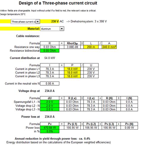
Some advanced PCB current calculators include the ability to calculate the voltage drop along a trace based on its length and current. This is particularly useful for power distribution traces, where excessive voltage drop can cause issues such as reduced performance or malfunctions in the connected components.
The voltage drop along a trace can be calculated using Ohm’s law:
V = I * R
Where:
– V is the voltage drop in volts
– I is the current flowing through the trace in amps
– R is the resistance of the trace in ohms
The resistance of a trace depends on its geometry and the resistivity of the copper material. The resistance can be calculated using the following equation:
R = ρ * L / A
Where:
– R is the resistance in ohms
– ρ (rho) is the resistivity of copper (1.68 x 10^-8 Ω·m at 20°C)
– L is the length of the trace in meters
– A is the cross-sectional area of the trace in square meters
By combining these equations, an advanced PCB current calculator can help you determine the maximum trace length for a given current and acceptable voltage drop.
Thermal Management and Cooling
In some cases, the current carrying capacity of a PCB trace may be limited by the ability of the PCB to dissipate heat. If the heat generated by the trace cannot be effectively removed, it can lead to thermal runaway and trace failure.
Advanced PCB current calculators may include thermal management features to help you design PCBs with adequate cooling. These features may include:
- Calculating the power dissipation of the trace based on the current and resistance
- Estimating the temperature rise of the PCB based on the power dissipation and the thermal properties of the PCB material
- Recommending cooling solutions, such as copper pours, thermal vias, or heatsinks, based on the calculated temperature rise
By using these advanced features, you can ensure that your PCB design can handle the required current without exceeding the thermal limits of the materials and components.
Best Practices for PCB Trace Current Design
Use Appropriate Trace Widths
When designing PCB traces, it’s essential to use appropriate trace widths for the expected current. Trace widths that are too narrow can lead to excessive heating, voltage drop, and reliability issues. On the other hand, traces that are too wide can waste board space and increase the overall PCB size and cost.
To determine the appropriate trace width, start by using a PCB current calculator to estimate the minimum width required for the expected current and temperature rise. Then, consider adding a safety margin of 20% to 50% to account for variations in manufacturing and operating conditions.
For example, if the calculator suggests a minimum trace width of 8 mils for a given current, you might choose to use a 10 mil or 12 mil trace to provide additional headroom and reliability.
Use Thicker Copper for High-Current Traces
In addition to using appropriate trace widths, it’s also important to use thicker copper for high-current traces. As mentioned earlier, thicker copper traces have lower resistance and can handle higher currents without excessive heating.
For most low-power signal traces, 1 oz copper is sufficient. However, for power traces or high-current applications, consider using 2 oz or even 4 oz copper. Keep in mind that thicker copper will increase the PCB cost and weight, so it’s important to use it judiciously and only where necessary.
Optimize Trace Routing
The routing of PCB traces can also impact their current carrying capacity. When routing traces, follow these best practices to optimize their current capacity and reliability:
- Avoid sharp corners and use 45° or curved traces instead. Sharp corners can cause current crowding and localized heating.
- Provide adequate spacing between traces to minimize crosstalk and thermal coupling. The spacing should be at least 2-3 times the trace width.
- Use ground planes and power planes to provide low-impedance return paths and improve heat dissipation.
- Minimize the length of high-current traces to reduce voltage drop and power loss.
- Use multiple vias to connect traces on different layers, as this can help distribute the current and reduce the resistance.
By following these best practices, you can design PCB traces that are optimized for current capacity, reliability, and performance.
Consider Thermal Management
As mentioned earlier, thermal management is crucial for ensuring the reliability and longevity of PCB traces. When designing high-current PCBs, consider incorporating thermal management features such as:
- Copper pours: Adding large copper areas, known as copper pours, can help spread the heat generated by the traces and improve heat dissipation.
- Thermal vias: Using thermal vias to connect traces to the ground or power planes can provide additional heat sinking and reduce the temperature rise.
- Heatsinks: For high-power applications, using heatsinks can help dissipate the heat generated by the traces and components.
- Airflow: Providing adequate airflow over the PCB can help remove heat and reduce the temperature rise.
By incorporating these thermal management features, you can design PCBs that can handle high currents without exceeding the thermal limits of the materials and components.
FAQ
What is a PCB current calculator?
A PCB current calculator is a tool that helps determine the maximum current a PCB trace can carry based on its width, thickness, temperature rise, and ambient temperature.
Why is it important to use a PCB current calculator?
Using a PCB current calculator ensures that your PCB traces are sized appropriately to handle the required current without overheating or failing prematurely. This is critical for the reliability and longevity of the PCB and the overall electronic device.
What factors affect the current carrying capacity of a PCB trace?
The current carrying capacity of a PCB trace depends on several factors, including the trace width, trace thickness, acceptable temperature rise, and ambient temperature.
How does copper weight affect the current capacity of a PCB trace?
Copper weight refers to the thickness of the copper layer on the PCB. Higher copper weights provide higher current capacity but also increase the PCB cost and weight. Common copper weights include 0.5 oz, 1 oz, 2 oz, 3 oz, and 4 oz per square foot.
What are some best practices for designing high-current PCB traces?
Some best practices for designing high-current PCB traces include using appropriate trace widths, using thicker copper for high-current traces, optimizing trace routing, and considering thermal management techniques such as copper pours, thermal vias, heatsinks, and airflow.
Conclusion
In this comprehensive article, we have explored the world of PCB current calculators and their importance in designing reliable and efficient PCBs. We have covered the basic concepts, factors affecting current capacity, advanced calculator features, and best practices for PCB trace current design.
By understanding how to use a PCB current calculator and applying the principles discussed in this article, you can design PCBs that are optimized for current capacity, reliability, and performance. Remember to always consider factors such as trace geometry, copper weight, temperature rise, and thermal management when designing high-current PCBs.
As technology continues to advance and electronic devices become more complex, the role of PCB current calculators will only become more critical. By staying up-to-date with the latest tools and best practices, you can ensure that your PCB designs are robust, efficient, and capable of meeting the demands of today’s electronics industry.

Leave a Reply