Introduction to PCB Prototypes
A Printed Circuit Board (PCB) prototype is an essential step in the development of electronic devices. It allows designers and engineers to test and validate their designs before mass production. PCB Prototypes are created to ensure that the circuit design functions as intended, and to identify any potential issues or improvements that need to be made.
In this article, we will dive into the world of PCB prototypes, exploring their importance, the different types of prototypes, and the process of creating them. We will also discuss the benefits of using PCB prototypes and some common challenges faced during the prototyping phase.
The Importance of PCB Prototypes
Verifying Design Functionality
One of the primary reasons for creating a PCB prototype is to verify that the design functions as intended. By building a physical prototype, designers can test the circuit in real-world conditions and ensure that it performs according to the specifications.
Identifying Design Flaws
PCB prototypes help identify any design flaws or weaknesses before mass production begins. It is much easier and cost-effective to make changes and improvements at the prototype stage rather than discovering issues after large quantities have been manufactured.
Testing Component Compatibility
Prototypes allow designers to test the compatibility of various components used in the circuit. This helps ensure that all components work together seamlessly and that there are no conflicts or interference issues.
Evaluating Manufacturing Processes
Creating a PCB prototype also helps evaluate the manufacturing processes involved. It allows manufacturers to assess the feasibility of the design, identify any potential production challenges, and optimize the manufacturing workflow.

Types of PCB Prototypes
Breadboard Prototype
A breadboard prototype is a quick and easy way to test a circuit design. It involves using a solderless breadboard to temporarily connect components and wires. Breadboard prototypes are ideal for initial concept testing and experimentation.
Perfboard Prototype
Perfboard prototypes are created by soldering components onto a perforated board. This type of prototype is more durable than a breadboard and allows for more permanent connections. Perfboard prototypes are suitable for more advanced testing and verification.
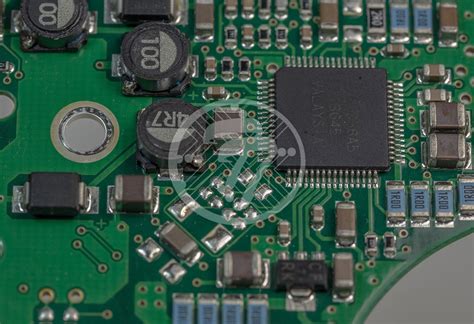
PCB Prototype
A PCB prototype is a fully functional circuit board that closely resembles the final product. It is created using the same materials and manufacturing processes as the final PCB. PCB prototypes are used for thorough testing, validation, and demonstration purposes.

The PCB Prototyping Process
Schematic Design
The first step in creating a PCB prototype is to design the schematic diagram. This involves defining the Circuit Components, their connections, and the overall functionality of the circuit. Schematic design is typically done using Electronic design Automation (EDA) software.
PCB Layout
Once the schematic is finalized, the next step is to create the PCB layout. This involves arranging the components on the board, routing the traces, and defining the board dimensions. PCB layout software is used to create the physical design of the board.
Fabrication
After the PCB layout is complete, the design files are sent to a PCB fabrication house. The fabrication process involves printing the circuit pattern onto a copper-clad board, etching away the unwanted copper, and applying a protective solder mask. The result is a bare PCB ready for component assembly.
Assembly
The final step in the PCB prototyping process is assembly. This involves soldering the components onto the fabricated PCB. Assembly can be done manually or using automated pick-and-place machines, depending on the complexity of the design and the quantity of prototypes required.

Benefits of Using PCB Prototypes
Cost Savings
Creating PCB prototypes helps save costs in the long run. By identifying and addressing design issues early in the development process, companies can avoid costly mistakes and rework during mass production.
Faster Time to Market
PCB prototypes enable faster iteration and refinement of the design. By quickly testing and validating the circuit, designers can make necessary changes and improvements, ultimately reducing the overall development time and bringing the product to market faster.
Improved Product Quality
Prototyping allows for thorough testing and validation of the PCB design. By identifying and resolving any quality issues during the prototype phase, companies can ensure that the final product meets the desired quality standards.
Enhanced Communication
PCB prototypes serve as tangible representations of the design, making it easier to communicate the concept to stakeholders, clients, and team members. They provide a clear visual understanding of the product and facilitate effective collaboration and feedback.
Common Challenges in PCB Prototyping
Design Complexity
As electronic devices become more advanced and sophisticated, PCB designs are becoming increasingly complex. Managing this complexity during the prototyping phase can be challenging, requiring careful planning and attention to detail.
Component Availability
Sourcing the required components for a PCB prototype can sometimes be a challenge. Certain components may have long lead times or may not be readily available in small quantities. This can impact the prototyping timeline and require careful supply chain management.
Manufacturing Constraints
PCB prototypes need to be designed with manufacturing constraints in mind. Factors such as minimum trace widths, hole sizes, and clearances must be considered to ensure that the design is manufacturable and meets the required specifications.
Testing and Debugging
Testing and debugging PCB prototypes can be time-consuming and complex, especially for high-density designs. Identifying and isolating faults requires specialized equipment and expertise. Effective testing strategies and thorough documentation are essential for successful debugging.
Frequently Asked Questions (FAQ)
1. How long does it take to create a PCB prototype?
The time required to create a PCB prototype depends on various factors, such as the complexity of the design, the availability of components, and the fabrication and assembly processes. On average, a simple PCB prototype can be created in a few days, while more complex designs may take several weeks.
2. How much does it cost to create a PCB prototype?
The cost of creating a PCB prototype varies depending on the size of the board, the number of layers, the components used, and the quantity of prototypes required. Simple PCB prototypes can cost a few hundred dollars, while more complex designs can cost several thousand dollars.
3. Can PCB prototypes be used for final production?
PCB prototypes are primarily used for testing and validation purposes and may not be suitable for final production. Prototypes may not have the same level of durability, reliability, or aesthetic finish as the final product. However, the knowledge gained from prototyping is invaluable in refining the design for mass production.
4. What is the difference between a PCB prototype and a proof-of-concept (POC)?
A POC is a simplified version of the design that demonstrates the basic functionality and feasibility of the concept. It may not include all the features or components of the final product. On the other hand, a PCB prototype is a fully functional representation of the final product, incorporating all the necessary components and features.
5. Can PCB prototypes be outsourced to third-party manufacturers?
Yes, PCB prototypes can be outsourced to specialized PCB fabrication and assembly houses. Outsourcing can be beneficial in terms of access to advanced manufacturing capabilities, faster turnaround times, and cost-effectiveness. However, it is important to choose a reputable and experienced manufacturer to ensure the quality and reliability of the prototypes.
Conclusion
PCB prototypes play a crucial role in the development of electronic devices. They allow designers and engineers to test and validate their designs, identify potential issues, and make necessary improvements before mass production. By investing in PCB prototyping, companies can save costs, reduce development time, and ensure the quality and reliability of their products.
Creating a PCB prototype involves several steps, including schematic design, PCB layout, fabrication, and assembly. Each step requires careful planning, attention to detail, and consideration of manufacturing constraints. While PCB prototyping can present challenges such as design complexity, component availability, and testing and debugging, the benefits far outweigh the challenges.
As technology continues to advance and electronic devices become more sophisticated, the importance of PCB prototyping will only continue to grow. By embracing the prototyping process and leveraging its benefits, companies can stay ahead of the competition, bring innovative products to market faster, and deliver high-quality solutions to their customers.
| Advantages of PCB Prototyping | Challenges in PCB Prototyping |
|---|---|
| Verifying design functionality | Design complexity |
| Identifying design flaws | Component availability |
| Testing component compatibility | Manufacturing constraints |
| Evaluating manufacturing processes | Testing and debugging |
| Cost savings | |
| Faster time to market | |
| Improved product quality | |
| Enhanced communication |
In conclusion, PCB prototyping is an essential step in the development of electronic devices. It enables designers and engineers to validate their designs, identify issues, and make improvements before committing to mass production. By embracing the PCB prototyping process and addressing the challenges it presents, companies can create high-quality, reliable products that meet the needs of their customers and stay competitive in the ever-evolving world of electronics.


Leave a Reply