Understanding PCB Safe Distance and Its Importance
When designing and manufacturing printed circuit boards (PCBs), one critical factor to consider is the PCB safe distance. This term refers to the minimum spacing required between various elements on a PCB, such as traces, pads, and components, to ensure proper functionality, reliability, and manufacturability. Maintaining appropriate safe distances helps prevent short circuits, signal interference, and manufacturing defects.
In this article, we will dive deep into the concept of PCB safe distance, exploring its significance, the factors that influence it, and the best practices for implementing safe distances in your PCB Designs. By understanding and adhering to these guidelines, you can create robust and reliable PCBs that meet industry standards and perform optimally in their intended applications.
Why PCB Safe Distance Matters
Maintaining proper safe distances on a PCB is crucial for several reasons:
-
Preventing short circuits: When conductive elements are too close together, there is a risk of unintended electrical connections or short circuits. This can lead to malfunctions, damage to components, or even complete failure of the PCB.
-
Reducing signal interference: Insufficient spacing between traces can result in electromagnetic interference (EMI) or crosstalk, which can distort or corrupt signals. This is particularly important for high-speed or sensitive circuits.
-
Ensuring manufacturability: PCB manufacturers have specific requirements for minimum feature sizes and spacings. Violating these requirements can result in manufacturing defects, reduced yield, or increased production costs.
-
Enhancing reliability: Proper safe distances help ensure the long-term reliability of the PCB by reducing the risk of electrical or mechanical issues that can arise from inadequate spacing.
Factors Influencing PCB Safe Distance
Several factors come into play when determining the appropriate safe distances for a PCB design:
-
PCB manufacturing process: Different PCB manufacturing processes have varying capabilities and limitations. For example, the minimum feature sizes and spacings achievable through standard etching processes may differ from those possible with advanced processes like high-density interconnect (HDI) or microvias.
-
PCB layer count: As the number of layers in a PCB increases, the safe distance requirements may change. Multilayer boards often have more stringent spacing requirements to accommodate the increased complexity and density of the design.
-
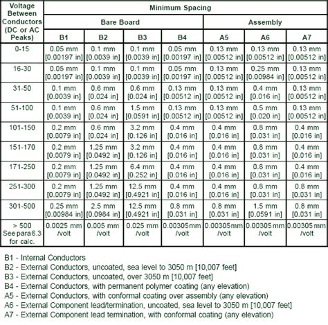
Operating voltage: The voltage levels present on the PCB can influence the required safe distances. Higher voltages generally demand greater spacings to prevent arcing or breakdown of insulation.
-
Environmental factors: The intended operating environment of the PCB can impact safe distance requirements. For example, PCBs exposed to harsh conditions, such as high humidity or extreme temperatures, may need increased spacings to maintain reliability.
-
Signal integrity: High-speed or high-frequency signals are more susceptible to interference and may require greater separation from other signals or components to maintain signal integrity.
PCB Safe Distance Guidelines
To ensure proper PCB safe distances, designers should follow established guidelines and standards. While the specific requirements may vary depending on the factors mentioned above, here are some general guidelines to consider:
Trace-to-Trace Spacing
The minimum spacing between traces on a PCB depends on several factors, such as the PCB material, copper thickness, and the voltage difference between the traces. As a general rule, the following table provides a starting point for trace-to-trace spacing based on the voltage difference:
| Voltage Difference | Minimum Spacing |
|---|---|
| <15V | 0.2 mm (8 mil) |
| 15V – 30V | 0.3 mm (12 mil) |
| 30V – 50V | 0.6 mm (24 mil) |
| 50V – 100V | 1.0 mm (40 mil) |
| 100V – 150V | 1.5 mm (60 mil) |
Note that these values are approximate and may need to be adjusted based on the specific requirements of your design and the PCB manufacturer’s capabilities.
Pad-to-Pad Spacing
The spacing between component pads on a PCB is crucial for ensuring proper soldering and preventing short circuits. The minimum pad-to-pad spacing depends on the component package type and the PCB manufacturing process. Here are some common guidelines:
| Component Package | Minimum Spacing |
|---|---|
| Surface Mount (SMD) | 0.2 mm (8 mil) |
| Through-Hole (THT) | 0.5 mm (20 mil) |
| Ball Grid Array (BGA) | 0.3 mm (12 mil) |
Again, these values are approximate and may need to be adjusted based on the specific component requirements and PCB manufacturer capabilities.
Copper-to-Board-Edge Spacing
Maintaining a safe distance between copper features (traces, pads, or planes) and the edge of the PCB is important for preventing damage during handling or assembly. The minimum spacing depends on the PCB Thickness and the copper feature type. As a general rule, the following guidelines apply:
| PCB Thickness | Minimum Spacing |
|---|---|
| <1.6 mm | 0.5 mm (20 mil) |
| ≥1.6 mm | 1.0 mm (40 mil) |
These values may need to be increased for high-voltage applications or if the PCB will be subjected to mechanical stress.

Best Practices for Implementing PCB Safe Distances
To ensure your PCB design adheres to safe distance requirements, consider the following best practices:
-
Consult with your PCB manufacturer: Engage with your PCB manufacturer early in the design process to understand their specific capabilities and requirements for safe distances. They can provide valuable guidance based on their experience and the manufacturing processes they use.
-
Use design rule checks (DRC): Most PCB design software includes DRC tools that automatically verify your design against a set of predefined rules, including safe distance checks. Configure these rules according to your specific requirements and run DRC regularly to catch any violations.
-
Consider the PCB Stack-Up: When designing a Multilayer PCB, carefully plan the stack-up to ensure appropriate spacing between layers. This includes considering the dielectric thickness, copper weight, and the spacing between adjacent layers.
-
Use copper pours and ground planes: Incorporating copper pours and ground planes in your PCB design can help maintain consistent spacing between traces and components, as well as provide shielding against EMI.
-
Plan for component placement: Arrange components on the PCB in a way that allows for sufficient spacing between them. Consider the size and orientation of each component, as well as the routing of traces between them.
-
Optimize trace routing: Route traces efficiently to minimize the overall trace length and avoid unnecessary crossovers or overlaps. This can help reduce the risk of signal integrity issues and maintain safe distances.
-
Document and communicate requirements: Clearly document the safe distance requirements for your PCB design and communicate them to all stakeholders, including the design team, manufacturers, and assemblers. This helps ensure everyone is working towards the same goals and reduces the risk of errors or misunderstandings.

Frequently Asked Questions (FAQ)
-
What happens if I violate PCB safe distance requirements?
Violating PCB safe distance requirements can lead to various issues, such as short circuits, signal integrity problems, manufacturing defects, and reduced reliability. In some cases, the PCB may not function as intended or may fail prematurely. -
Can I use smaller safe distances to save space on my PCB?
While it may be tempting to use smaller safe distances to reduce the overall size of your PCB, it is generally not recommended. Violating safe distance requirements can compromise the integrity and reliability of your design. If space is a concern, consider using advanced PCB manufacturing processes or optimizing your component placement and routing. -
How do I determine the safe distance requirements for my specific PCB design?
The safe distance requirements for your PCB design depend on various factors, such as the PCB manufacturing process, layer count, operating voltage, and signal integrity requirements. Consult with your PCB manufacturer and refer to industry standards and guidelines to determine the appropriate safe distances for your specific design. -
What tools can I use to ensure my PCB design adheres to safe distance requirements?
Most PCB design software includes design rule check (DRC) tools that can verify your design against a set of predefined rules, including safe distance checks. These tools can help identify any violations and ensure your design adheres to the specified requirements. Additionally, engaging with your PCB manufacturer and leveraging their expertise can help ensure your design meets their specific guidelines. -
Can I use different safe distances for different parts of my PCB?
Yes, it is possible to use different safe distances for different parts of your PCB, depending on the specific requirements of each area. For example, you may need to use larger spacings for high-voltage sections or critical signal paths, while other areas may allow for tighter spacings. However, it is important to clearly communicate these variations in your design documentation and ensure they are properly implemented during manufacturing.

Conclusion
PCB safe distance is a critical aspect of PCB design that ensures proper functionality, reliability, and manufacturability. By understanding the factors that influence safe distances and adhering to established guidelines and best practices, you can create robust and reliable PCBs that meet industry standards and perform optimally in their intended applications.
Remember to consult with your PCB manufacturer, leverage design rule checks, and carefully plan your PCB stack-up, component placement, and trace routing to maintain appropriate safe distances. By prioritizing PCB safe distance throughout the design process, you can minimize the risk of issues and ensure the success of your PCB projects.


Leave a Reply