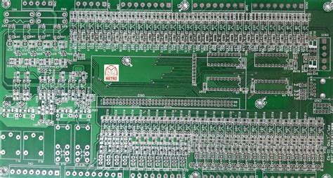
Introduction to PCB-PTHs”>PCB-PTHs
Plated Through Holes (PTHs) are a critical component in the design and manufacturing of Printed Circuit Boards (PCBs). PCB-PTHs are holes drilled through a PCB that are then plated with a conductive material, typically copper, to create electrical connections between different layers of the board. These connections allow signals and power to be routed vertically through the board, enabling more complex circuit designs and higher component density.
PCB-PTHs are essential for several reasons:
- They provide electrical connections between layers in a multi-layer PCB.
- They allow components to be mounted on both sides of the board.
- They enhance the mechanical strength of the board by reinforcing the connection between layers.
In this article, we will dive deeper into the world of PCB-PTHs, exploring their types, manufacturing process, design considerations, and best practices.
Types of PCB-PTHs
There are several types of PCB-PTHs, each with its own characteristics and applications:
Through Hole PTHs
Through Hole PTHs are the most common type of PTHs. They are drilled completely through the board and plated with copper to create an electrical connection between layers. Through Hole PTHs are typically used for mounting through-hole components, such as resistors, capacitors, and connectors.
Blind Via PTHs
Blind Via PTHs are holes that are drilled from one side of the board to an inner layer, but do not go all the way through the board. They are used to create connections between the outer layer and an inner layer of the PCB. Blind Via PTHs are commonly used in high-density PCB designs where space is limited.
Buried Via PTHs
Buried Via PTHs are holes that are drilled between two inner layers of a multi-layer PCB, without connecting to either of the outer layers. They are used to create connections between inner layers of the board, allowing for more complex routing and higher component density. Buried Via PTHs are typically used in advanced PCB designs with multiple layers.
Micro Via PTHs
Micro Via PTHs are very small holes, typically less than 0.15mm in diameter, that are used to create high-density interconnects between layers. They are commonly used in HDI (High Density Interconnect) PCBs, where space is at a premium and high component density is required. Micro Via PTHs are usually laser-drilled to achieve the small diameter and high precision required.

PCB-PTH Manufacturing Process
The manufacturing process for PCB-PTHs involves several steps:
-
Drilling: Holes are drilled through the PCB substrate using a CNC drilling machine. The diameter and location of the holes are determined by the PCB design.
-
Deburring: After drilling, the holes are deburred to remove any rough edges or debris that may interfere with the plating process.
-
Cleaning: The board is cleaned to remove any contaminants or residues that may affect the plating process.
-
Copper Deposition: A thin layer of copper is deposited onto the walls of the holes using an electroless plating process. This creates a conductive base layer for the subsequent plating steps.
-
Electroplating: The board is then electroplated with additional copper to increase the thickness of the copper layer in the holes. This step ensures a reliable electrical connection and mechanical strength.
-
Finishing: Finally, the board undergoes a finishing process, such as solder mask application and surface finish (e.g., HASL, ENIG, or OSP), to protect the copper and prepare the board for component assembly.

PCB-PTH Design Considerations
When designing PCBs with PTHs, several factors must be considered to ensure optimal performance and manufacturability:
Hole Diameter
The diameter of the PTHs is a critical design parameter. It must be large enough to accommodate the component leads or wires that will be inserted into the holes, but not so large that it unnecessarily consumes board space. The hole diameter also affects the manufacturability of the board, as smaller holes are more difficult and expensive to drill and plate.
Plating Thickness
The thickness of the copper plating in the PTHs is another important consideration. It must be thick enough to provide a reliable electrical connection and mechanical strength, but not so thick that it unnecessarily increases the cost and complexity of the manufacturing process. Typical plating thicknesses range from 20-50 microns, depending on the application and requirements.
Pad Size and Shape
The size and shape of the pads surrounding the PTHs are also important design factors. The pads must be large enough to provide a sufficient area for soldering the component leads, but not so large that they consume unnecessary board space. The shape of the pads can also affect the solderability and reliability of the connections.
Via Spacing and Placement
The spacing and placement of PTHs on the board must be carefully considered to ensure proper signal integrity and avoid interference between adjacent vias. The spacing between vias should be sufficient to prevent signal crosstalk and maintain the required impedance of the traces. The placement of vias should also be optimized to minimize the length of the traces and reduce signal reflections.

PCB-PTH Best Practices
To ensure the best performance and reliability of PCB-PTHs, several best practices should be followed:
- Use appropriate hole diameters for the component leads or wires.
- Ensure sufficient copper plating thickness for reliable electrical and mechanical connections.
- Optimize pad sizes and shapes for solderability and reliability.
- Maintain proper via spacing and placement to ensure signal integrity and avoid interference.
- Follow the manufacturer’s recommendations for drilling, plating, and finishing processes.
- Use appropriate test methods, such as microsectioning and impedance testing, to verify the quality and reliability of the PTHs.
By following these best practices, designers and manufacturers can ensure that their PCBs with PTHs will perform reliably and meet the required specifications.
PCB-PTH Quality Control
Quality control is critical in the manufacturing of PCBs with PTHs. Several methods are used to ensure the quality and reliability of the PTHs:
Visual Inspection
Visual inspection is the first line of defense in quality control. The board is visually inspected for any obvious defects, such as missing or misaligned holes, incomplete plating, or damage to the board surface.
Microsectioning
Microsectioning is a destructive testing method that involves cutting a cross-section of the board and examining it under a microscope. This allows the plating thickness, hole wall quality, and other internal features of the PTHs to be directly measured and evaluated.
Impedance Testing
Impedance testing is a non-destructive testing method that measures the electrical impedance of the PTHs and traces on the board. This helps to ensure that the PTHs have the correct electrical characteristics and are properly connected to the traces.
Continuity and Isolation Testing
Continuity testing verifies that there is a continuous electrical path between the intended points on the board, while isolation testing ensures that there are no unintended short circuits between adjacent traces or vias. These tests are typically performed using automated test equipment (ATE) that can quickly test a large number of points on the board.
Frequently Asked Questions (FAQs)
- What is the difference between a Through Hole PTH and a Blind Via PTH?
-
A Through Hole PTH goes completely through the board, while a Blind Via PTH only goes from one side of the board to an inner layer, but not all the way through.
-
What is the purpose of copper plating in PTHs?
-
Copper plating in PTHs serves two main purposes: (1) it creates a conductive pathway for electrical signals to travel between layers of the board, and (2) it provides mechanical reinforcement to the hole, making the board more robust.
-
How small can Micro Via PTHs be?
-
Micro Via PTHs can be as small as 0.1mm in diameter, although 0.15mm is a more common lower limit. The exact size depends on the capabilities of the manufacturing process and the requirements of the PCB design.
-
What is the typical plating thickness for PTHs?
-
The typical plating thickness for PTHs ranges from 20-50 microns (0.02-0.05mm). The exact thickness depends on the requirements of the PCB design and the manufacturing process used.
-
Why is quality control important for PCB-PTHs?
- Quality control is important for PCB-PTHs because defects in the holes, such as incomplete plating, can lead to electrical failures or mechanical weaknesses in the board. Thorough testing and inspection help to ensure that the PTHs meet the required specifications and will perform reliably in the final application.
Conclusion
Plated Through Holes (PTHs) are a critical component in the design and manufacturing of Printed Circuit Boards (PCBs). They provide electrical connections between layers, allow components to be mounted on both sides of the board, and enhance the mechanical strength of the board. There are several types of PTHs, each with its own characteristics and applications, including Through Hole PTHs, Blind Via PTHs, Buried Via PTHs, and Micro Via PTHs.
The manufacturing process for PCB-PTHs involves drilling, deburring, cleaning, copper deposition, electroplating, and finishing steps. Designers must consider several factors when incorporating PTHs into their PCB designs, including hole diameter, plating thickness, pad size and shape, and via spacing and placement.
To ensure the best performance and reliability of PCB-PTHs, several best practices should be followed, including using appropriate hole diameters, ensuring sufficient plating thickness, optimizing pad sizes and shapes, maintaining proper via spacing and placement, following manufacturer’s recommendations, and using appropriate test methods for quality control.
Quality control methods for PCB-PTHs include visual inspection, microsectioning, impedance testing, and continuity and isolation testing. These methods help to ensure that the PTHs meet the required specifications and will perform reliably in the final application.
By understanding the types, manufacturing process, design considerations, best practices, and quality control methods for PCB-PTHs, designers and manufacturers can create high-quality, reliable PCBs that meet the demands of today’s complex electronic devices.


Leave a Reply