What is Solder mask clearance?
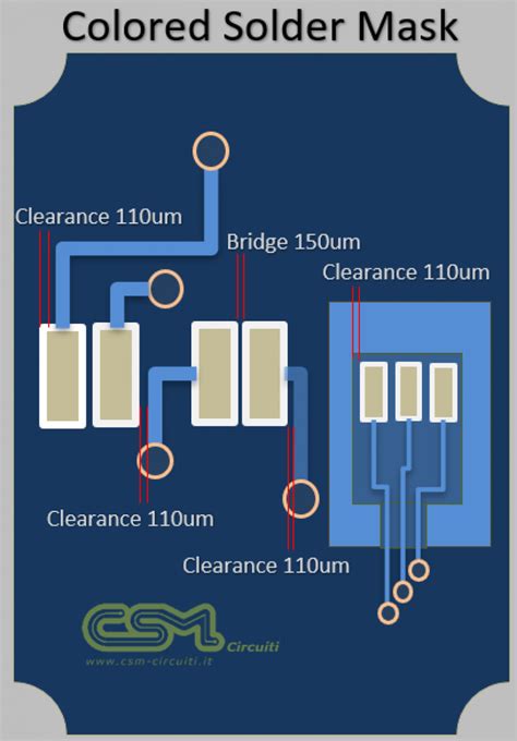
Solder mask clearance refers to the minimum distance between the edge of a drilled hole (such as a via or through-hole) and the edge of the solder mask opening around that hole on a printed circuit board (PCB). This clearance is an important design parameter that helps ensure the manufacturability, reliability, and functionality of the PCB.
In PCB Design, solder mask is a thin lacquer-like layer of polymer that is applied over the copper traces on the board. Its primary purpose is to protect the copper from oxidation, prevent solder bridges from forming between closely spaced pads, and provide electrical insulation. Solder mask also serves as a barrier to limit the flow of solder during the assembly process, helping to create more reliable solder joints.
Importance of Solder Mask Clearance
Proper solder mask clearance is crucial for several reasons:
-
Manufacturing Tolerance: During PCB Fabrication, there can be slight variations in the positioning of drilled holes and the application of solder mask. Adequate clearance ensures that these manufacturing tolerances do not result in the solder mask encroaching on the hole, which could lead to issues during assembly or operation.
-
Solder Wicking: If the solder mask opening is too close to the hole, there is a risk of solder wicking up the hole during reflow. This can cause problems such as solder starved joints, inconsistent solder joint formation, or even short circuits between layers in multi-layer boards.
-
Mechanical Stress: Components subjected to mechanical stress or vibration can transmit those forces to the PCB through the solder joints. If there is Insufficient Solder mask clearance, the solder joint may be weaker and more prone to cracking or failure under stress.
-
Electrical Clearance: In high-voltage applications, the solder mask provides necessary electrical insulation and creepage distance. Proper clearance helps maintain this insulation and prevents arcing or leakage currents.
Tented Vias and Solder Mask Clearance
Tented vias are holes in a PCB that are completely covered by solder mask on one or both sides of the board. This is in contrast to non-tented or exposed vias, where the hole is left open. Tenting of vias is commonly used for several purposes:
-
Protection: Tented vias help prevent contamination or debris from entering the hole, which could cause issues with reliability or signal integrity.
-
Solder Wicking Prevention: By covering the via with solder mask, the risk of solder wicking into the hole during assembly is greatly reduced.
-
Electrical Insulation: Tented vias provide an additional layer of electrical insulation between the via and any components or traces on the surface of the PCB.
-
Aesthetic Appearance: Tented vias create a cleaner, more uniform appearance on the surface of the PCB, which can be desirable for some applications.
When using tented vias, it is important to consider the solder mask clearance to ensure proper coverage of the hole without encroaching on the barrel or causing manufacturing issues.
Recommended Solder Mask Clearance for Tented Vias
The specific solder mask clearance requirements for tented vias can vary depending on the PCB manufacturer, the fabrication process, and the design requirements of the board. However, there are general guidelines that are widely used in the industry.
IPC Standards
The IPC (Association Connecting Electronics Industries) is a global trade association that develops standards for the electronic interconnection industry. IPC-6012, the “Qualification and Performance Specification for Rigid Printed Boards,” provides guidance on solder mask clearances.
According to IPC-6012 Class 2 (which covers most standard commercial PCBs), the minimum solder mask clearance for tented vias is 0.05 mm (0.002 in) from the edge of the hole to the edge of the solder mask opening. For more demanding applications, such as IPC Class 3 (which includes high-reliability aerospace and medical devices), the minimum clearance is increased to 0.075 mm (0.003 in).
| IPC Class | Minimum Solder Mask Clearance |
|---|---|
| Class 1 | Not specified |
| Class 2 | 0.05 mm (0.002 in) |
| Class 3 | 0.075 mm (0.003 in) |
It’s important to note that these are minimum values, and many PCB designers and manufacturers will choose to use larger clearances to provide additional margin for manufacturing tolerances and to enhance reliability.
Typical Manufacturer Recommendations
While IPC standards provide a baseline, individual PCB manufacturers may have their own recommended solder mask clearances based on their specific processes and capabilities. It’s always a good idea to consult with your chosen manufacturer early in the design process to ensure that your clearances meet their guidelines.
Many manufacturers recommend a minimum solder mask clearance of 0.1 mm (0.004 in) for tented vias, which provides a balance between reliable coverage and ease of manufacturing. Some may suggest larger clearances, such as 0.15 mm (0.006 in) or even 0.2 mm (0.008 in), for high-reliability applications or to accommodate their specific processes.
| Manufacturer | Recommended Solder Mask Clearance |
|---|---|
| Manufacturer A | 0.1 mm (0.004 in) |
| Manufacturer B | 0.15 mm (0.006 in) |
| Manufacturer C | 0.2 mm (0.008 in) |
Design Considerations
When designing your PCB, it’s important to consider the impact of solder mask clearance on other aspects of your layout. Some key considerations include:
-
Via Size: The solder mask clearance is measured from the edge of the drilled hole, not the edge of the copper pad surrounding the hole. When choosing your via sizes, make sure to account for the solder mask clearance to ensure that the solder mask opening will not encroach on the copper pad.
-
Trace Spacing: If you have traces running between tented vias, ensure that there is sufficient space between the traces and the solder mask openings to prevent any potential short circuits or manufacturing issues.
-
Component Placement: When placing components near tented vias, consider the solder mask clearance to avoid any interference with the component pads or solder joints.
-
Thermal Relief: If your tented vias are connected to large copper pours (such as ground or power planes), you may need to add thermal relief pads around the via to prevent solder wicking and ensure reliable soldering. The size and spacing of these thermal relief pads should also take into account the solder mask clearance.
FAQ
1. What happens if the solder mask clearance is too small?
If the solder mask clearance is too small, several issues can arise:
– The solder mask may encroach on the drilled hole, leading to manufacturing defects or difficulty in plating the hole.
– Solder wicking may occur during reflow, causing solder to flow up the hole and potentially creating short circuits or poor solder joint formation.
– The solder joint may be weaker and more susceptible to cracking or failure under mechanical stress.
2. Can I use different solder mask clearances on different parts of my PCB?
Yes, it is possible to specify different solder mask clearances for different areas of your PCB, depending on the specific requirements of your design. For example, you may choose to use larger clearances for high-voltage areas or smaller clearances for dense component areas. However, it’s important to communicate these requirements clearly to your PCB manufacturer and ensure that they are able to accommodate your design.
3. Are there any disadvantages to using tented vias?
While tented vias offer several benefits, there are a few potential disadvantages to consider:
– Tented vias can make it more difficult to inspect the solder joints visually, as the solder is hidden under the solder mask.
– If the solder mask is damaged or begins to peel away, it can expose the via and potentially lead to contamination or reliability issues.
– In some high-frequency applications, tented vias may create small capacitances that can impact signal integrity, although this is typically only a concern for very high-speed designs.
4. How do I choose the right solder mask clearance for my PCB?
Choosing the right solder mask clearance depends on several factors, including:
– The requirements of your specific application (e.g., high-reliability, high-voltage, etc.)
– The capabilities and recommendations of your chosen PCB manufacturer
– The density and complexity of your PCB layout
– Any relevant industry standards or guidelines (such as IPC)
It’s always best to consult with your PCB manufacturer early in the design process to ensure that your chosen clearances are appropriate and manufacturable.
5. Can I use tented vias on both sides of my PCB?
Yes, tented vias can be used on one or both sides of a PCB, depending on the design requirements. In some cases, vias may be tented on one side and exposed on the other, while in others, they may be fully tented on both sides. The choice depends on factors such as the board’s intended use, the environment it will operate in, and any assembly or manufacturing considerations.

Conclusion
Solder mask clearance is a critical design parameter for PCBs, particularly when using tented vias. By providing sufficient clearance between the edge of the drilled hole and the edge of the solder mask opening, designers can ensure reliable manufacturing, prevent solder wicking, and enhance the mechanical and electrical integrity of the board.
When Choosing Solder mask clearances for tented vias, it’s important to consider industry standards, manufacturer recommendations, and the specific requirements of your application. By working closely with your PCB manufacturer and following best design practices, you can create a robust, reliable PCB that meets the needs of your project.

Leave a Reply