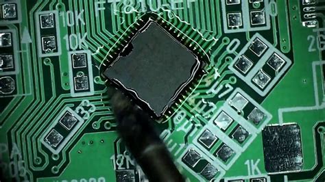
Introduction to QFN Packages and Soldering Challenges
Quad Flat No-lead (QFN) packages have become increasingly popular for integrated circuits due to their small size, low profile, and good thermal and electrical performance. However, the small pitch and hidden leads underneath the package make QFNs more challenging to solder reliably compared to traditional leaded packages like QFP or SOIC.
Proper PCB Board layout is critical for achieving reliable soldering of QFN packages in volume production. This article will discuss best practices and guidelines for designing PCB landing pads and soldermask for robust QFN assembly.
Key Challenges in QFN Soldering
Some of the main difficulties in soldering QFN packages include:
- Small pitch (0.4mm, 0.5mm, 0.65mm are common)
- Leads are hidden underneath the package (not visible for inspection)
- Thermal Pad requires extra solder volume for good bonding
- Prone to soldering defects like opens, shorts, voiding if not optimized
Careful PCB Design is needed to ensure the right amount of solder is applied to each lead and the thermal pad makes good contact for reliability.
PCB Footprint Layout for QFN Soldering
Land Pattern Dimensions
The landing pad size and spacing should be based on the specific QFN package drawing. In general, the pad should extend 0.2-0.5mm beyond the lead on each side to allow for registration tolerance.
A typical land pattern for a 0.5mm pitch QFN might have:
| Dimension | Typical Value |
|---|---|
| Pad width | 0.3mm |
| Pad length | 0.8mm |
| Pad spacing | 0.5mm |
The stencil aperture for each pad is usually made slightly smaller, around 0.2mm narrower than the copper pad.
Thermal Pad
A unique aspect of QFNs is the large thermal pad underneath the center of the package. This pad is important for conducting heat out of the IC and into the PCB. Solder paste must be printed on the thermal pad area to form a good solder bond.
There are a few different approaches to the thermal pad stencil pattern:
- Large opening covering most of thermal pad
- Array of smaller openings (50-75% coverage)
- Segmented pad with separate paste deposits
Option 1 is simplest but most prone to voiding. Option 3 is most complex to design but provides the best control over solder volume.
Segmentation example:
| Opening Size | Pitch |
|---|---|
| 1.5mm x 1.5mm square | 1.8mm |
The segmented openings allow outgassing during reflow to minimize voiding. Thermal vias should be used under the thermal pad to further improve heat transfer.
Soldermask Design
Solder mask is important for preventing solder bridges between pads. The mask openings should be 1:1 with the copper pads or slightly larger (0.05mm per side).
For the thermal pad, a large opening can be used or the segmented pads can be connected with mask channels to allow outgassing. The webbing should be at least 0.15mm wide.
Example soldermask pattern:
| Opening | Dimensions |
|---|---|
| Lead pads | 0.35 x 0.85mm (1:1 with copper) |
| Thermal pad | 4.0 x 4.0mm opening with 0.2mm webbing |

Stencil Design for QFN
Stencil thickness and aperture dimensions are critical for achieving the right solder paste volume. If too little paste is printed, opens can occur. If too much, shorts and excessive voiding are likely.
Stencil Thickness
A typical stencil thickness for QFNs is 0.1mm (4 mils) to 0.125mm (5 mils). Thinner stencils are sometimes used for finer pitch (<0.5mm).
| Pitch | Typical Stencil |
|---|---|
| 0.5mm | 0.125mm (5 mil) |
| 0.4mm | 0.100mm (4 mil) |
Aperture Size
The stencil aperture should be 1:1 with the land pattern or slightly smaller. Home plate shaped apertures are commonly used.
Recommendations:
| Pad Size | Aperture Size |
|---|---|
| 0.25mm | 0.20mm |
| 0.30mm | 0.25mm |
| 0.40mm | 0.35mm |
For the thermal pad, an array of square openings at 50-75% coverage is typical. Apertures of 1.0-2.0mm spaced 0.5-1.5mm apart are a good starting point.
Stencil Material
Laser-cut stainless steel stencils are most commonly used. Electroform nickel stencils can achieve finer features for ultra-fine pitch components.
Nano-coated stencils are becoming popular to improve paste release. This is especially important for small apertures in QFN designs.

Reflow Profile Optimization
The reflow profile should be optimized to achieve good wetting and minimize voiding, especially under the thermal pad. In general, a higher peak temperature and longer time above liquidus (TAL) is beneficial.
Recommended profile:
| Parameter | Value |
|---|---|
| Peak Temperature | 245-250°C |
| Time Above Liquidus (217°C) | 60-90 seconds |
Linear ramp rates of 1-2°C/second are preferred to minimize ΔT across the assembly. Soak time can be extended to 120-180 seconds for larger boards.
Nitrogen reflow atmosphere can further reduce the risk of voiding by limiting oxidation. 100-1000ppm residual O2 content is typical.

Inspection and Quality Control
Post-reflow inspection is important to verify soldering quality of QFNs. However, visual inspection is limited since the leads are hidden under the package.
X-Ray Inspection
X-ray inspection is the most effective method to verify solder joint quality and check for common defects:
- Opens or poor wetting
- Shorts or excess solder
- Voiding under thermal pad
2D X-ray is suitable for basic inspection, but computed tomography (CT) provides more detailed visualization of defects in 3D.
Inspection criteria example:
| Defect | Acceptance Criteria |
|---|---|
| Solder Short | None allowed |
| Thermal Pad Voiding | <25% single void, <40% total |
| Open | Not allowed |
Electrical Test
Boundary scan testing and flying probe are useful electrical techniques to detect opens and shorts that may not be visible on X-ray.
Manufacturing defect analysis (MDA) should be performed on a sample of assemblies to monitor quality and correct any systematic issues.
Common Defects and Solutions
Some common assembly issues with QFNs include:
1. Opens or Poor Wetting
Caused by:
– Insufficient Solder volume
– Poor Land Pattern Design
– Oxidized pads or contamination
Solutions:
– Increase stencil aperture size or thickness
– Optimize land pattern geometry
– Verify proper cleaning and plating of PCB pads
2. Solder Shorts
Caused by:
– Excess solder paste
– Stencil misalignment
– Poorly defined solder mask
Solutions:
– Reduce stencil aperture dimensions
– Improve stencil printing registration
– Enlarge solder mask webbing between pads
3. Thermal Pad Voiding
Caused by:
– Outgassing during reflow
– Poor wetting or contamination
– Non-optimized thermal pad pattern
Solutions:
– Segment thermal pad stencil openings
– Increase reflow TAL and peak temperature
– Use no-clean flux and avoid cleaning agents
FAQs
Q1: What is a typical land pattern size for a 0.5mm pitch QFN?
A1: For a 0.5mm QFN, a typical pad size is 0.3mm x 0.8mm with 0.5mm spacing between pads.
Q2: How much solder paste should be printed on the thermal pad?
A2: A common goal is 50-75% solder paste coverage on the thermal pad using an array of 1.0-2.0mm square openings.
Q3: What type of stencil is best for printing solder paste on QFNs?
A3: Laser-cut stainless steel stencils with a thickness of 0.100-0.125mm are commonly used. Electroformed nickel and nano-coated stencils are also options for finer features.
Q4: What reflow profile is recommended for QFN soldering?
A4: A linear ramp to a peak of 245-250°C with 60-90 seconds above liquidus (217°C) is a good starting point. Nitrogen atmosphere can help reduce voiding.
Q5: How can soldering defects like opens and shorts be detected on QFNs?
A5: X-ray inspection is the most effective method to check for opens, shorts, and voids under the hidden leads of the QFN. Boundary scan and flying probe electrical tests can also detect some defects not visible on X-ray.
Conclusion
Reliable QFN soldering requires careful PCB land pattern and stencil design along with an optimized reflow profile. Key considerations include:
- Precise landing pad dimensions based on package size
- Segmented thermal pad pattern with adequate solder coverage
- Solder mask webbing to prevent shorts
- Optimized stencil apertures and paste transfer
- Higher reflow peak temperature and TAL to minimize voiding
By following best practices and monitoring quality with X-ray inspection and electrical testing, high yields can be achieved with these advanced packages.


Leave a Reply