Introduction to Solder paste printing in SMT Assembly
Solder paste printing is a critical step in surface mount technology (SMT) assembly, which involves depositing solder paste onto printed circuit boards (PCBs) to establish electrical connections between components. This process is essential for ensuring the reliability and functionality of electronic devices in various industries, such as consumer electronics, automotive, aerospace, and medical equipment.
In this comprehensive article, we will delve into the fundamentals of solder paste and its role in SMT assembly. We will also discuss the solder paste printing process, including the equipment, techniques, and best practices for achieving optimal results. Additionally, we will address common challenges and solutions in solder paste printing, as well as the latest advancements in this field.
What is Solder Paste?
Solder paste is a homogeneous mixture of tiny solder particles suspended in a flux medium. It is a critical material used in SMT assembly to form electrical and mechanical connections between surface mount components and PCB pads. The composition of solder paste typically includes the following:
- Solder alloy particles (e.g., tin-lead, lead-free)
- Flux (e.g., rosin, no-clean, water-soluble)
- Rheological additives (e.g., thickeners, stabilizers)
- Solvents
The solder alloy particles are responsible for forming the actual solder joint, while the flux removes oxides and other contaminants from the surfaces to be soldered, promoting better wetting and adhesion. The rheological additives help to control the flow properties and printability of the solder paste, while the solvents maintain the desired consistency and prevent premature drying.
Types of Solder Paste
Solder paste comes in various types, each with specific characteristics and applications. The most common types include:
-
Lead-based solder paste: Contains tin-lead alloys (e.g., Sn63Pb37), which have a lower melting point and better wetting properties compared to lead-free alternatives. However, due to environmental and health concerns, lead-based solder paste is being phased out in many countries.
-
Lead-free solder paste: Uses lead-free alloys (e.g., SAC305 – Sn96.5Ag3.0Cu0.5) to comply with RoHS regulations. Lead-free solder paste has a higher melting point and requires tighter process control compared to lead-based solder paste.
-
No-clean solder paste: Formulated with a flux that leaves minimal residue after reflow, eliminating the need for post-soldering cleaning. No-clean solder paste is widely used in SMT assembly due to its convenience and cost-effectiveness.
-
Water-soluble solder paste: Contains a flux that can be easily removed with water after reflow. This type of solder paste is preferred when a clean PCB surface is required, such as in high-reliability applications or when conformal coating is necessary.
Solder Paste Properties
The performance of solder paste in SMT assembly is determined by several key properties, including:
-
Particle size distribution: The size and distribution of solder particles affect the printability, slump resistance, and reflow behavior of the solder paste. Smaller particles (e.g., Type 4, Type 5) are used for fine-pitch components, while larger particles (e.g., Type 3) are suitable for standard SMD sizes.
-
Viscosity: The viscosity of solder paste influences its flow properties and ability to maintain the printed pattern. A well-balanced viscosity ensures good printability, slump resistance, and tack time.
-
Flux activity: The flux in solder paste must effectively remove oxides and promote wetting during reflow. The activity level of the flux should be chosen based on the Surface Finishes, component types, and environmental conditions.
-
Shelf life: Solder paste has a limited shelf life, typically ranging from 3 to 6 months when stored at room temperature. Proper storage conditions (e.g., refrigeration) can extend the shelf life and maintain the paste’s quality.

Solder Paste Printing Process
Solder paste printing is the process of depositing solder paste onto PCB pads through a stencil using a printing machine. The main steps involved in solder paste printing are as follows:
-
Stencil preparation: A stencil is a thin metal sheet (e.g., stainless steel, nickel) with apertures that match the PCB pad layout. The stencil thickness and aperture size are determined by the solder paste type, component sizes, and PCB Design. Proper stencil cleaning and maintenance are crucial for consistent print quality.
-
Solder paste loading: Solder paste is placed on the stencil surface, typically using an automated dispenser or manual application. The amount of solder paste should be sufficient to cover the stencil apertures without excessive waste.
-
Printer setup: The PCB is aligned with the stencil using fiducial marks and camera systems. The printing parameters, such as squeegee pressure, speed, and separation distance, are adjusted based on the solder paste type, stencil design, and PCB characteristics.
-
Printing cycle: The squeegee blade moves across the stencil, forcing the solder paste through the apertures and onto the PCB pads. The printing process can be performed in a single direction or with multiple passes, depending on the solder paste properties and desired print quality.
-
Stencil cleaning: After printing, the stencil is cleaned to remove any residual solder paste and prevent contamination. Stencil cleaning can be done using manual methods (e.g., wiping with solvents) or automated systems (e.g., understencil cleaning machines).
-
Inspection: The printed PCB is inspected visually or using automated solder paste inspection (SPI) systems to detect any defects, such as insufficient paste, bridging, or misalignment. SPI systems provide quantitative data on paste volume, height, and area, enabling process control and quality assurance.
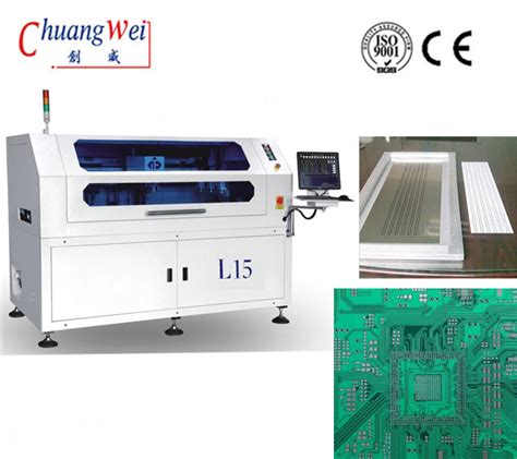
Solder Paste Printing Equipment
Solder paste printing equipment includes various types of printers, stencils, and accessories that are designed to optimize the printing process and ensure consistent results. The main categories of solder paste printing equipment are:
-
Solder paste printers: These machines are used to deposit solder paste onto PCBs through a stencil. Solder paste printers can be manual, semi-automatic, or fully automatic, with features such as vision alignment, closed-loop process control, and multi-lane capability. The choice of printer depends on factors such as production volume, PCB complexity, and budget.
-
Stencils: Stencils are thin metal sheets with apertures that match the PCB pad layout. They are used to control the amount and placement of solder paste on the PCB. Stencils can be made from different materials (e.g., stainless steel, nickel) and fabricated using various methods (e.g., laser cutting, electroforming). The stencil design, including aperture size, shape, and orientation, is critical for achieving optimal print quality.
-
Understencil cleaning systems: These systems are used to clean the bottom side of the stencil during the printing process, removing any residual solder paste and preventing contamination. Understencil cleaning can be performed using dry wipes, vacuum nozzles, or solvent-based methods. Automated understencil cleaning systems are integrated into solder paste printers for efficient and consistent cleaning.
-
Solder paste inspection (SPI) systems: SPI systems are used to inspect the printed solder paste on PCBs, providing quantitative data on paste volume, height, and area. These systems use 2D or 3D imaging techniques to detect defects and measure paste deposits, enabling process control and quality assurance. SPI data can be used to optimize the printing parameters and identify potential issues before component placement.
Solder Paste Printing Techniques
Solder paste printing techniques refer to the methods and practices used to achieve optimal print quality and consistency. Some key techniques include:
-
Stencil design optimization: The stencil design should be optimized based on the PCB Layout, component sizes, and solder paste properties. This includes selecting the appropriate aperture sizes, shapes, and orientations, as well as incorporating features such as stepped stencils or relief cavities to improve paste release and prevent bridging.
-
Printer parameter optimization: The printing parameters, such as squeegee pressure, speed, and separation distance, should be optimized for the specific solder paste, stencil, and PCB characteristics. This can be done through a design of experiments (DOE) approach, where different parameter combinations are tested and evaluated based on print quality metrics.
-
Print-on-demand (PoD): PoD is a technique where solder paste is dispensed directly onto the stencil apertures, rather than using a conventional flood and squeegee method. PoD systems use a pressurized cartridge and nozzle to deposit solder paste, reducing waste and improving print consistency, especially for high-mix, low-volume production.
-
Stencil cleaning optimization: Proper stencil cleaning is essential for maintaining print quality and preventing defects. The cleaning frequency, method, and materials should be optimized based on the solder paste type, printing volume, and environmental conditions. Automated understencil cleaning systems can improve cleaning efficiency and consistency.
-
Process control and monitoring: Implementing process control and monitoring techniques, such as statistical process control (SPC) and real-time SPI feedback, can help to identify and correct printing issues before they impact product quality. This involves collecting and analyzing data on key print parameters and defects, setting control limits, and taking corrective actions when necessary.

Challenges and Solutions in Solder Paste Printing
Solder paste printing is a complex process that can be affected by various factors, such as solder paste properties, stencil design, PCB characteristics, and environmental conditions. Some common challenges and solutions in solder paste printing are:
-
Insufficients: Insufficient Solder paste on PCB pads can lead to weak or open solder joints, affecting the reliability of the assembled device. Causes of insufficients include clogged stencil apertures, low squeegee pressure, or poor paste release. Solutions include optimizing the stencil design, adjusting printing parameters, and improving stencil cleaning.
-
Bridging: Bridging occurs when solder paste deposits connect adjacent PCB pads, causing short circuits. Causes of bridging include oversized stencil apertures, high squeegee pressure, or poor paste rheology. Solutions include optimizing the stencil design, adjusting printing parameters, and using solder paste with better slump resistance.
-
Poor wetting: Poor wetting refers to the inability of molten solder to adhere to PCB pads or component leads during reflow, resulting in weak or non-existent solder joints. Causes of poor wetting include oxidation, contamination, or incompatible surface finishes. Solutions include using solder paste with appropriate flux activity, ensuring proper storage and handling of materials, and implementing adequate cleaning processes.
-
Stencil life: Stencils are subject to wear and tear during the printing process, leading to reduced print quality and consistency over time. Causes of stencil degradation include abrasion, deformation, or clogging of apertures. Solutions include using durable stencil materials (e.g., nickel), implementing proper stencil cleaning and storage procedures, and monitoring stencil performance using SPI data.
-
Environmental factors: Solder paste printing can be affected by environmental factors, such as temperature, humidity, and airborne contamination. These factors can influence the rheology, tackiness, and shelf life of solder paste, as well as the print quality and consistency. Solutions include controlling the printing environment (e.g., using air filtration and humidity control systems), monitoring paste condition using SPI data, and adjusting printing parameters based on environmental changes.

Latest Advancements in Solder Paste Printing
The field of solder paste printing is continuously evolving, driven by the demand for smaller, more complex electronic devices and the need for higher efficiency and reliability in SMT assembly. Some of the latest advancements in solder paste printing include:
-
Jet printing: Jet printing is an emerging technology that uses piezoelectric or pneumatic actuators to dispense solder paste directly onto PCB pads, without the need for a stencil. This allows for greater flexibility in PCB design, as well as the ability to print on non-planar surfaces and accommodate last-minute design changes. Jet printing also reduces solder paste waste and enables the printing of smaller features compared to traditional stencil printing.
-
Nanocoating stencils: Nanocoating is a process where a thin layer of material (e.g., fluoropolymer) is applied to the stencil surface and aperture walls to improve solder paste release and reduce clogging. Nanocoated stencils exhibit better print definition, consistency, and longevity compared to uncoated stencils, especially for fine-pitch applications and lead-free solder paste.
-
Closed-loop SPI feedback: Closed-loop SPI feedback involves integrating SPI data with the solder paste printer’s control system to automatically adjust printing parameters in real-time. This enables the printer to compensate for variations in paste condition, stencil wear, and environmental factors, ensuring consistent print quality and reducing the need for manual intervention.
-
Artificial intelligence (AI) and machine learning (ML): AI and ML techniques are being applied to solder paste printing to improve process control, defect detection, and quality prediction. By analyzing large datasets from SPI systems, AI/ML algorithms can identify patterns and correlations that may not be apparent to human operators, enabling proactive process optimization and reducing the risk of defects.
-
Sustainable solder paste formulations: With the increasing emphasis on environmental sustainability, solder paste manufacturers are developing formulations that are more eco-friendly and comply with international regulations (e.g., RoHS, REACH). This includes the use of lead-free alloys, biodegradable flux, and recyclable packaging materials. Sustainable solder paste formulations aim to reduce the environmental impact of SMT assembly while maintaining or improving performance.
Frequently Asked Questions (FAQ)
-
What is the shelf life of solder paste, and how should it be stored?
Solder paste typically has a shelf life of 3 to 6 months when stored at room temperature (25°C/77°F). To extend the shelf life and maintain the paste’s quality, it is recommended to store solder paste in a refrigerator at 2-10°C (36-50°F) and allow it to reach room temperature before use. Solder paste should be kept in sealed containers to prevent contamination and moisture absorption. -
What is the difference between lead-based and lead-free solder paste?
Lead-based solder paste contains tin-lead alloys (e.g., Sn63Pb37), which have a lower melting point and better wetting properties compared to lead-free alternatives. However, due to environmental and health concerns, lead-based solder paste is being phased out in many countries. Lead-free solder paste uses lead-free alloys (e.g., SAC305 – Sn96.5Ag3.0Cu0.5) to comply with RoHS regulations and has a higher melting point and requires tighter process control compared to lead-based solder paste. -
How often should I clean my stencil during solder paste printing?
The frequency of stencil cleaning depends on various factors, such as the solder paste type, printing volume, and environmental conditions. As a general guideline, it is recommended to clean the stencil every 1-4 hours of continuous printing or every 20-50 prints, whichever comes first. However, this can be adjusted based on the specific process requirements and the level of contamination observed during printing. -
What are the common defects in solder paste printing, and how can they be prevented?
Common defects in solder paste printing include insufficients (low paste volume), bridging (paste connecting adjacent pads), poor wetting (incomplete solder joint formation), and solder balls (small spheres of solder on the PCB surface). These defects can be prevented by optimizing the stencil design, adjusting printing parameters (e.g., squeegee pressure, speed), improving stencil cleaning, using appropriate solder paste formulations, and controlling environmental factors (e.g., temperature, humidity). -
How can I optimize my solder paste printing process?
To optimize your solder paste printing process, consider the following steps:
a. Select the appropriate solder paste type and particle size for your application
b. Design and maintain a high-quality stencil with optimized aperture sizes and shapes
c. Set up and calibrate your solder paste printer according to the manufacturer’s guidelines
d. Determine the optimal printing parameters through experimental testing and statistical analysis
e. Implement a robust stencil cleaning and maintenance procedure
f. Monitor the printing process using SPI systems and statistical process control (SPC) techniques
g. Regularly train and educate operators on best practices and troubleshooting methods
Conclusion
Solder paste printing is a critical step in SMT assembly that directly impacts the quality and reliability of electronic devices. By understanding the fundamentals of solder paste, the printing process, and the challenges involved, engineers and operators can optimize their workflows and achieve consistent, high-quality results.
As the electronics industry continues to


Leave a Reply