Introduction to PCB GERBER Files
PCB GERBER files are the standard file format used in the PCB industry for manufacturing printed circuit boards. These files contain all the necessary information required to fabricate a PCB, including the copper layers, solder mask, silkscreen, and drill data. GERBER files are named after their creator, H. Joseph Gerber, who developed the format in the 1960s.
What are PCB GERBER Files?
PCB GERBER files are a set of ASCII vector format files that describe the layout of a printed circuit board. Each file represents a specific layer of the PCB, such as the top copper layer, bottom copper layer, solder mask, and silkscreen. These files are generated by PCB Design software and are used by PCB Manufacturers to create the physical boards.
Why are PCB GERBER Files Important?
PCB GERBER files are essential for PCB manufacturing because they provide a standardized format for communicating PCB design information between designers and manufacturers. Without GERBER files, it would be challenging to ensure that the manufactured PCB matches the designer’s intent. Additionally, GERBER files allow for greater accuracy and precision in PCB Fabrication, which is crucial for modern electronic devices.
Understanding the Structure of PCB GERBER Files
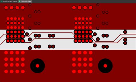
Layers in PCB GERBER Files
A typical set of PCB GERBER files consists of several layers, each representing a specific aspect of the PCB design. These layers include:
- Top Copper Layer (.GTL)
- Bottom Copper Layer (.GBL)
- Top Solder Mask (.GTS)
- Bottom Solder Mask (.GBS)
- Top Silkscreen (.GTO)
- Bottom Silkscreen (.GBO)
- Drill Data (.DRL)
Each layer is described using a series of commands and coordinates that define the geometry of the PCB features.
Apertures and D-Codes
In PCB GERBER files, apertures and D-Codes are used to define the shape and size of the features on each layer. Apertures are the basic building blocks of GERBER files and are defined at the beginning of the file using the AD command followed by a unique D-Code number and the aperture’s shape and size.
For example:
%ADD10C,0.5*%
This command defines an aperture with D-Code 10, which is a circular shape with a diameter of 0.5 units.
Throughout the GERBER file, D-Codes are used to reference the defined apertures when drawing features on the PCB Layers.
Coordinates and Commands
PCB GERBER files use a coordinate system to specify the location of features on the PCB. The coordinates are typically expressed in inches or millimeters and are relative to the origin (0,0) of the PCB.
Various commands are used to control the plotter and draw features on the PCB layers. Some common commands include:
G01: Linear interpolation (draw a line)G02: Clockwise circular interpolation (draw an arc)G03: Counterclockwise circular interpolation (draw an arc)G36: Begin polygon area fillG37: End polygon area fillM02: End of file
These commands, along with the coordinates and D-Codes, define the geometry of the PCB features on each layer.

The Process of Reverse Engineering PCB GERBER Files
Reverse engineering PCB GERBER files involves analyzing the files to extract design information and recreate the PCB Layout in a design software. This process can be useful for understanding the structure and functionality of an existing PCB, making modifications, or creating documentation.
Step 1: Obtain the PCB GERBER Files
To reverse engineer a PCB, you first need to obtain the GERBER files for the board. These files may be available from the original designer, the manufacturer, or they may need to be generated from a physical PCB using a process called “PCB digitization.”
Step 2: Import the GERBER Files into PCB Design Software
Once you have the GERBER files, import them into a PCB design software that supports the GERBER format. Popular software options include:
- Altium Designer
- KiCad
- Eagle
- OrCAD
- Cadence Allegro
Most PCB design software have built-in tools for importing GERBER files and reconstructing the PCB layout.
Step 3: Analyze the PCB Layers
After importing the GERBER files, carefully examine each PCB layer to understand the layout and components of the board. Pay attention to the following aspects:
- Component placement
- Trace routing
- Vias and through-holes
- Power and ground planes
- Solder mask and silkscreen
Take notes on the board’s structure and any unique features that may be present.
Step 4: Identify Components and Create a Bill of Materials (BOM)
Using the silkscreen layer and your knowledge of electronic components, identify the components used on the PCB. Create a bill of materials (BOM) that lists each component, its value, package type, and quantity. This information will be useful if you plan to recreate the PCB or need to source replacement components.
Step 5: Reconstruct the Schematic
Based on the PCB layout and the identified components, reconstruct the schematic for the circuit. This step requires an understanding of electronic circuits and the ability to recognize common circuit patterns. Use the PCB design software’s schematic editor to create a schematic that represents the circuit on the PCB.
Step 6: Validate and Document the Design
Compare the reconstructed schematic and PCB layout with the original GERBER files to ensure accuracy. Make any necessary corrections or adjustments to the design. Once the design is validated, create documentation that includes:
- The reconstructed schematic
- The PCB layout
- The bill of materials (BOM)
- Any additional notes or observations about the design
This documentation will be valuable for future reference or if the PCB needs to be modified or reproduced.

Applications of Reverse Engineering PCB GERBER Files
Reverse engineering PCB GERBER files has several applications in the electronics industry, including:
Legacy System Maintenance and Repair
Many older electronic systems may not have complete documentation or the original design files. By reverse engineering the PCB GERBER files, technicians can understand the system’s structure and components, making it easier to maintain, repair, or upgrade the system.
Competitive Analysis
Companies may reverse engineer a competitor’s PCB to understand their design techniques, component choices, and manufacturing processes. This information can be used to improve their own products or gain a competitive advantage in the market.
Design Modification and Optimization
Reverse engineering a PCB can help identify areas for improvement, such as optimizing component placement, reducing the board size, or enhancing signal integrity. By understanding the existing design, engineers can make informed decisions about modifying the PCB for better performance or cost-effectiveness.
Education and Training
Reverse engineering PCB GERBER files can be a valuable learning tool for students and new engineers. By analyzing real-world PCB designs, they can gain practical experience in PCB layout, component selection, and circuit analysis. This hands-on experience can complement theoretical knowledge and prepare them for future design challenges.

Challenges in Reverse Engineering PCB GERBER Files
Despite the benefits of reverse engineering PCB GERBER files, there are several challenges that engineers may face during the process:
Incomplete or Inaccurate GERBER Files
In some cases, the available GERBER files may be incomplete or contain errors. This can make it difficult to reconstruct the PCB layout accurately and may require additional investigation or assumptions about the design.
Complex or Proprietary Components
Some PCBs may contain complex or proprietary components that are difficult to identify or source. In such cases, reverse engineering the PCB may require extensive research or collaboration with component manufacturers to determine suitable replacements or alternatives.
Intellectual Property Concerns
Reverse engineering a PCB may raise intellectual property concerns, particularly if the design is protected by patents or trade secrets. It is essential to ensure that any reverse engineering efforts comply with legal and ethical guidelines and respect the rights of the original designers.
Time and Resource Constraints
Reverse engineering a PCB can be a time-consuming and resource-intensive process, particularly for complex designs. Companies and engineers must carefully consider the costs and benefits of reverse engineering a PCB and allocate resources accordingly.
Best Practices for Reverse Engineering PCB GERBER Files
To successfully reverse engineer PCB GERBER files, consider the following best practices:
-
Use high-quality GERBER files: Ensure that the GERBER files used for reverse engineering are complete, accurate, and of high resolution to minimize errors and ambiguity.
-
Employ appropriate tools and software: Use reliable PCB design software and tools that support the GERBER format and have features for importing and analyzing GERBER files.
-
Document the process: Maintain detailed notes and documentation throughout the reverse engineering process, including observations, assumptions, and any challenges encountered.
-
Collaborate with experts: Consult with experienced PCB designers, component engineers, or industry experts when facing complex or unfamiliar aspects of the design.
-
Validate the results: Compare the reverse-engineered design with the original GERBER files and, if possible, with a physical PCB to ensure accuracy and completeness.
-
Respect intellectual property: Always ensure that reverse engineering efforts comply with legal and ethical guidelines and do not infringe upon the intellectual property rights of others.
Frequently Asked Questions (FAQ)
- What are the most common file extensions for PCB GERBER files?
- .GTL (Top Copper Layer)
- .GBL (Bottom Copper Layer)
- .GTS (Top Solder Mask)
- .GBS (Bottom Solder Mask)
- .GTO (Top Silkscreen)
- .GBO (Bottom Silkscreen)
-
.DRL (Drill Data)
-
Can I reverse engineer a PCB without the original GERBER files?
Yes, it is possible to reverse engineer a PCB without the original GERBER files by using a process called “PCB digitization.” This involves scanning or photographing the physical PCB and using specialized software to reconstruct the PCB layout. -
What is the difference between a schematic and a PCB layout?
A schematic is a symbolic representation of an electronic circuit, showing the components and their interconnections. A PCB layout, on the other hand, is the physical representation of the circuit on a printed circuit board, showing the actual component placement and trace routing. -
How accurate is reverse engineering a PCB from GERBER files?
The accuracy of reverse engineering a PCB from GERBER files depends on the quality and completeness of the files, as well as the skill and experience of the engineer performing the reverse engineering. In most cases, a high degree of accuracy can be achieved, but there may be some limitations or ambiguities in the reconstructed design. -
Is it legal to reverse engineer a PCB?
The legality of reverse engineering a PCB depends on the specific circumstances and the intended use of the reverse-engineered design. In general, reverse engineering for the purpose of interoperability, repair, or education is considered fair use. However, if the reverse engineering process infringes upon patents, trade secrets, or other intellectual property rights, it may be illegal. It is essential to consult with legal experts and ensure compliance with applicable laws and regulations.
Conclusion
Reverse engineering PCB GERBER files is a valuable skill in the electronics industry, enabling engineers to understand, modify, and reproduce existing PCB designs. By following a systematic approach and utilizing appropriate tools and techniques, engineers can successfully reconstruct PCB layouts and schematics from GERBER files.
However, reverse engineering PCBs also presents challenges, such as incomplete data, complex components, and intellectual property concerns. To overcome these challenges, engineers should adhere to best practices, collaborate with experts, and ensure compliance with legal and ethical guidelines.
As technology continues to advance and the demand for electronic devices grows, the ability to reverse engineer PCB GERBER files will remain an essential skill for engineers, technicians, and researchers in the field. By leveraging this skill, professionals can contribute to the development, maintenance, and optimization of electronic systems across various industries.


Leave a Reply