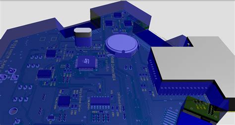
Introduction to PCB 3D Design
Printed Circuit Board (PCB) design has evolved significantly over the years, with the introduction of 3D functions playing a crucial role in enhancing the design process. PCB 3D design allows engineers and designers to visualize and optimize their designs in a three-dimensional space, leading to improved accuracy, efficiency, and overall product quality. In this article, we will explore the reasons behind the adoption of 3D functions in PCB Design and how they have revolutionized the industry.
The Need for 3D Visualization in PCB Design
As electronic devices become more complex and compact, the need for efficient and accurate PCB design has become paramount. Traditional 2D design methods often fall short in providing a comprehensive understanding of the PCB’s layout, component placement, and potential design issues. By incorporating 3D functions, designers can:
- Visualize the PCB from various angles and perspectives
- Identify potential conflicts between components and connectors
- Optimize component placement for better performance and space utilization
- Simulate and analyze the PCB’s thermal and mechanical properties
Benefits of Using 3D Functions in PCB Design
The use of 3D functions in PCB design offers numerous benefits, including:
-
Improved Accuracy: 3D visualization allows designers to identify and resolve potential issues early in the design process, reducing the risk of costly mistakes and redesigns.
-
Enhanced Collaboration: 3D models can be easily shared among team members, facilitating better communication and collaboration between designers, engineers, and manufacturers.
-
Faster Time-to-Market: By streamlining the design process and minimizing errors, 3D functions help reduce development time and accelerate product launches.
-
Cost Savings: Identifying and resolving issues early in the design process helps avoid expensive redesigns and manufacturing delays, ultimately leading to cost savings.
Key Features of PCB 3D Design Software
To effectively leverage the benefits of 3D functions in PCB design, engineers and designers rely on advanced software tools. These tools offer a range of features that enable efficient and accurate 3D modeling, simulation, and analysis. Some of the key features include:
3D Component Libraries
PCB 3D design software often includes extensive libraries of 3D component models, allowing designers to easily incorporate accurate representations of real-world components into their designs. These libraries include:
- Connectors
- Integrated Circuits (ICs)
- Capacitors and Resistors
- Heat Sinks and Cooling Solutions
Having access to a wide range of 3D component models ensures that designs accurately reflect the physical characteristics of the components, leading to more precise simulations and analyses.
3D Routing and Placement
Advanced PCB 3D design software offers intelligent routing and placement capabilities, allowing designers to optimize the layout of their PCBs in a three-dimensional space. These features include:
- Automatic and manual routing options
- Via and pad placement optimization
- Clearance and spacing checks
- Layer stackup management
By leveraging these capabilities, designers can create efficient and compact PCB Layouts while ensuring proper signal integrity and avoiding potential conflicts between components.
Thermal and Mechanical Analysis
One of the most significant advantages of using 3D functions in PCB design is the ability to perform thermal and mechanical analyses. These analyses help designers understand how the PCB will perform under various environmental conditions and identify potential issues related to Heat Dissipation and structural integrity. Some of the key analysis features include:
- Thermal simulation and heat map generation
- Structural analysis and stress testing
- Vibration and shock analysis
- Fluid dynamics simulation for cooling optimization
By conducting these analyses early in the design process, engineers can make informed decisions about component placement, cooling solutions, and material selection, ultimately leading to more reliable and robust PCBs.
 ECMSqo+RSM56uT1JrQeNWSVD92RGU/RlwajE4p1pWWx87icV9Yl/dX9XIte1Z4oPCOtWTiRNjRSKchJXtt1uQ2OcYH61xGJr+7lZEAaaR5WA+6gY5PWle0v0kS1aOXIdvLXkpk8Fh/D9a6TTdNSBMYyxGZH/vHHQe1dMI0sBS9x3etvS7a+6561fFQoU0oat7f5j9PsY4URQBtAyTgZdumTV53REUtgHOAM4yTxipQv8Aq1UckhFHqWIAAqcz2djHrem6nDJ9rkMawtCI5YwEzlfM6jnris8Lh5YmfNPY8ijTdaTcn6s0Pt954SuJ44oobuHUra3L/aAoYMqbhsMZPy8msCzeSS7mma3mb7Q5/wCPeLcUklkwNgbA5Py9aqRQzPGZBJnyzhQSzPuAyAowahku7yYsZbiZtzMzfOQCXfzG4HHJ56da+jkoxjyWPYowcmpRdktjaknzE/7kLvibBu7mNOWRpARGnJyAR9ePrkmW5sZ5BZ3O8R7UWaAP5b5w3G4A+vbtVb5eo656nrV3T5njnZckeYoGRuHKn2IP6/n0rOly09IqyOqpTlPWUtSyurXE5topHW0WSQLeT20W2Qx5O4jZ3I46d6r3RsTPL9hgMNoDthRiWcqON7k9z1NRSx+XLKmPuucZBBwee/NWLC3S7vbO1dyiTSqjsuCwUnnaG4z6V2RSXvHl1Kk5/u2T2wuDHZXF7576NBeokm4l4lfAJUJnPTrin3s1sLnUJLa4ZNKZjLJHHuSFmJOFSP8AKpJ5bq2W80XbEbVJnlE0gHmohyDuI+WueuJvtsixRArZwHCjoZG6bj9f89a561VQXMzeMVCN5bLf/IXfLfT+fIMRr8tvH2VB0rVji8uFpiVVFZU3Mcbnb+FR3Pem2VugDSSBRFGhZtxKggfwqQOtVbq5NwUEeRbxAiBPTcckn3968NN4io7jWDqV4qvPRPRLr6+gXE5kOxT+7U5/3j61Dk4IzxjH4U2lzjk9K9GEVBWR6MKcacVFDd7wsjL03AHnH4Yre0bWvK3mciIRnnJJBX+8KybGxudRS/uInhVLONWCyOA77mwfLX1xn/8AWaeIOzLwamVSUHzJaHFXm17yWh1OsajFMlpPG4dGgIUochvmzwRWLCAoluLpRtKlgsm4Fl9VplvbSzGC3D4jiV23OfkhjzuZj7D/AD1q/Gk2vTQ2aJtsrdizTkASGJTgFxjGW7f/AFq4MTUnXklFaMeEr0+bnqK9tl0b8yilwqyzX0g89UUyRK/ClUwEUgdh6V3R/facblyEM1sCi9cvJH90fnXOWWgG71i704OXs7KATXPRWeIlSFAH5Gtm8u0YqyDZa2qjylUcBEHXH4cV1YWEkm5GlGLjdvrqR6dHLbeGre2lGHF7KxGQersRyKydTK4gG4ZUuzAEfKMDrWveajb/ANmxXCYkRrhFAjIzuYHr/WuLvbglpQv35naSTHq3YVeJd4qjDrb7jlqz9qvZR6/kVrmYzOcfcXhRUQFKBTwK3p01Tjyo76dONOKjEaBS4p+KXFaGgzFLinYpcUAMxS4p2KXFADMUYp+KMUAMxRin4oxQAzFGKfijFADcUuKXFOxQAuKMU8ijFADMUYp+KMUAMxRin4oxQAzFGKfijFADMUYp+KMUAMxRin4oxQAzFGKdijFADQoJUZAyQMnoMnGTWt9mNqqqVwOu/gh/cEcVlEVPBeXNuNqMGiPWKQboz+B6fhXBjaFStFeze3Tv8zzcfh6teKVN7dO/zOdvtFuxdTGDY0ckrMOdpQMd3Oa2tP06O3jRRg8/vHwMuw5rTR9NuyAT9nlP8Ln923+6/wDjUrRPEAjqV6Ff7pHsRxXjYjEVnalUVrfj/n8jw8RiK8rUq2lvx/z+QzaBuXHGePbuKMU6krmirHLcrtbhizA46sR1/Kn4VAuOAq4+mKk6fkQfoakV5tKl0XVp4DLYyO8qJGw8xghMYc7gV68jNdOHw0sRUstjooUXUlZEXlwnS/7SguQl7bX2IkMiZjWNdwZoj82Sayry9ur+Y3N0VMrdSiBFyeTgLxUjxxX99cTQq8cLvuYvjdyc847mrF2ViSGIwq1u5WMbGAmV88bVI59+a+qgoUEoRR71PD80OWGi/MpQSbRKAcHhwcgEdVOCf8RVB+HcejH/AD0/pWjJZOjsbWRJGUfNEWw4BHfBzVEQMJpPtZMZDQkKwYZQko2AD24P4USfM7o6aSdKPLIQMP0qYS4eKQggRkbmPYEhCePrSotoEAO9iUCttUDloWibBPvtYfjU5nj2zhYV/fLMjFzuOJfLY4HqGXI+tONK7uE8RFaFlrRr29gt7J4ZpbhekZ2orKMnczIi9Papnmsn0uLTRG66hBdSuSEUBmbb83mjkjipRA2m2WjavYzK11IXMyuY5IyS2AgjHP1zWTqF5KjSKu0391zKUGBChHQe9aSkoryOWMdXJ7v8iteTs5NlA5YZzdTZJLkcbc+gqeztGYxxxqSSQEHr7k1BaWwUAde7H1NaRmNtFcBMBpoXgB/iAcjJX8sfjXh1avt6iXQ5ZT9tNQjsF/eRywjT0UNFbso89fl8xgPmwPT0/wDr1nfypBS110qUaStE99Sk4pSewYqMQ3V19oW2hmnW2iee5EAyyxJ1PPFJPLsXAIBPBJPCj1NbME0ehIyxX/2iy1PS0nwkW3NwCMorYz0JAzitUuZ2MZu/uodfGzie0l0e1jhW40lbd977ZMNskWSUgYLdcn/Cq0DtNPGhIISM7iOAzAcmqexU2BDKXMSR/vGLFEHIjAPpV60jaLDjrz17561liqyguVdTixdZQjyLdlt96JNApAW5SOOT1KrIHwD7nGa7Sy09NOtkgUfMcNLIB998fyHQVxp3ysmxGLKCSFBbheScCuyXWLeP7L57CMXFtDKA3zJuOdwJx9K4cPiKcaqhN6vRfi2cmEly3k+hHoG5fEHipyDg6auD26isq5OLS6PpA/8AKuth+yGK7uYMAy20iNtbKEbSeK4DUbxWVVhm/ciNhLtPyuxIwM+2K9Gs1Qpd73/E7amIUYNrd7GdLMsUKkdW5UH16ZrOGWJJ5J5NOd2kbJ6DhR6CnKtZ4elyRvLdlYah7KOu7ADj+VKBSgZp4FdZ2IbilxTsUuKBjcUYp2KXFADMUuKdijFADcUYp2KMUANxRinYpcUAMxRin4oxQAzFLinYpcUAOxSYp5FGKAGYoxT8UmKAG4oxT8UYoAZijFPxSYoAbijFOxS4oAZijFOxRigBuKMU7FGKAIyKaRUpFIAM8/nQIi21Zgvbq2ATIkiPPlS/MmPbuKjKEc9R6imEdKxqU4VVyzV0YVKcKseWaujVjmsrnARvIlP/ACzmPyE/7D/40rpJGdrqVPbPf6GscirUF9cwARkiWHvHL8w/4Ceorya2WyjrRd/J/o/8/vPFr5Y460X8n+j/AM/vJ5lYPBFOs8UM67xIEx5qdP3RbCn35pt7f3dxDDpX2tZdOscmCSSNEaOLhiJGHp061v6br1s1sunXFvb3Vjk/6FehQybjuP2efGPpn9KwNXOl2d3PFb28o066MRjimDefEzD5kctwQDypBPHevQwdenCHskrS7Pe/fz+RthIwbVJ+6+qej/ya80VYZ2iRXVWSBmUQxsn72Rez7eu9/wCEdhzVu4tZxBaT3EluZpZsCzwyyQqT/rILlCVJUcyZA9s9yIQu7zCQyP0G45MY6EAe/f8A+tVVY7m8uXjIIYsiGJjglD8ywJ7HG6Vvw7V0X11PdSSVkXoNPtneMgDdEWme4kY7lXqzyOvUe30FZ+qX326SO2tI2+y2+/YMAyOe8j47nr+nbldSvvs0QsLWbd8xku516yy+ijsi9FH496rWV5EMi6gLHAMc1uVjlVwWbdKpG1s556cDjpWsIS3RhVqwXuyZAox+HX2rdsP+JHdW1xqMJMN7YyGIw+XKyCZSqlgcgH9RTdK0+HWTq7Sy7ZYLXzbdFkjj3Pnq2/qAPSoZ9Qu57WF9SeN4LAGGDaiq87KSFXI610OWmpwRhrzL5FSeSCyWW4VTvmdjZwt1AP8Ay0YVRtoJHYySEtLIdzseTzSr513O11N958eWvZF7AewrSijCL+v/ANevExeI53yR2OevV/5dx+YAJEhJ4AHNUpJGkYsenRR6CnTzeY21fuL09z61CCD0IP0rTD0eRc0tz0MJh/ZrmluLTZJAi57nhR6mlLBQSeg5qe00+W8s9R1KO7jhmsQrWsYCyO8i/vPmU9BgcHHX6V0PeyOyUraLcuadbW8Eet22q6ewu5rGOaJ7oDy1glz8yDqGzjnPHTjvRSS7SK2SVoysNusMITJzgk7zmrOoX0Oqz+czSsRaokrqzIshc7yhH1qCJDI6nHAwFHYAcfpTqVI0YXOarUVGF2Pt4Szbmz7/AOFXxx9KaqhQAP8A9daOm28Er3n2mNmVLCeeEZZAXXADAjqK+er1+VOpM8WKlWn5st2cL2LlnljLXujXNxGqE7lRsDDZ/WuTufEKTHQIYG80rbRW96JEKlZdwX5T+tXNc1m4tI/Dd3brGWuNFlgZZcttjlC8jB6jFczpNm09xFM3+rjkUgd2cHP5VOCw908VX+XquZf5HsSjToUGpbHdWd7dWqTrbzsqsjrIh5XDAg/Kawp5AxEafcTj64qe4mZPNRTy5Gcegqqq16uFhKaU59NjjwVBv95P5Aq9Kk2kcfjUkcfQn8KVh8x/CvSR6yGAU4CnAU7FMoZilxTsUuKAGYpcU7FGKAG4oxTsUYoAbijFOxRigBuKMU7FLigBmKMU7FGKAG4pcU7FLigBSKMU4ijFADcUYp2KMUANoxTsUYoAbijFOxRigBuKMU7FGKAG4oxTsUYoAZijFOxRigBmKQipMUmKBEfI6cU4KHzxggZ46H8KXFAyORweR+dJoTRGUI+nqOlNxUoyOn/66MIf9k/pS1J1RBtqVpJJY1gnzLEpygY/PGTxlH6igoR2/HtSYwQfQg1Moxna6IlGMtWhggcc2zl9o+452zL9D3/X6Vf0walqc8unW8eJ5YmzLhRMUXJaKPcQuTxzkVSYckj1zU8F28LBnRZOnzElJlx0KSr8wNTNzirpc34MmUqkIvlV/wACK58O6pbwRTahavb/ADFZHLKTCy5+WVQe/UcYPY1Xs7OSRwY4J54Y2VpjEhLeUDluB7V2ttr6XkH2PUoY9VtGABhuysd/GBzmOYYDY9yD71DLoNs6S3XhvVCBAGmuLC9Hl3luo5ZhkZIH0/E1eHxlObcdpdnozhlWhXko7NdOv3dvQzddbQ9S1BbzTmkjtIrdTdyPGIVQKMBEC4rmp5W1CfhSlpD8kEfbg9T7nvV7UsyCGytiRaqzNO/eaTuxP8v/AK1LBbqgXjAHQelcuMxaiuSDMa+IUFaL95/gXdB02O9luHkYiG1ZFKpgM8nXBJH3RWlrmj2wsb25ty8UgQmQbt0bhzsOFPQ88YrC0+6kstSu40uvs5mAZN8DTwSEDcRIqsGHsQDVbV/EmqToI1mVVEhQrBGUXPK5YuSfXFaUVT9mrI9OjSgqUWlpZHMpc3EZeCSU+VuKFsbmABx8p61pWz2pDCEnGed3fHGRVRLWGY4O9XOAhXnJPbFdfZ+CpPsi+bciK4Yb8YLIoI4UgDr68mtd/hNue690wB8xFxJDcSWFvNCt20A5VXbHLHgZ5xWpqBjgvb46XDBBFd28CuqkqIyuQG289R1/+vUc5utIttU0m8YNG0imFY1AZzKAD8w69iP6VVVArNhnd3Ch3kbcxCjAFJe4m2JtRTlIk+aQqv8ACuB/n61eijCDpz39vao7eLaAx/D/ABqz0B+lePXrOrK/Q8GvWdWV+hPbWk139q8tkUW9u9xIZDj5VIGBjvU+p6zbWMujyTysLefw/NCmxS4Mm1NnTt1q4UtbK5uLWASf6T4ce5kZ2By3ybsfnXm15qN3qSaXbSJGPsVutpD5YOXAOAWz36V5uHo/Xql38C++zT/VHr4Wj7KPNLcr28U13LHEC5Uf3iSI0zkgV1sMUdlAoCgHaAg7gH1qtpliltCWcgt95z2Leg9hU8rNI2SeMcV7DbxVXlXwo423jKv91EXzMxY8k1Kq8Z9KFTpU5UBMe4r1UrKyPVS6D2AVU/3RUWCTn1pxLNjJzgYFKBVFCAUuKdilxQMbijFOxRigBuKMU7FLigBuKMU7FGKAG4oxTsUYoAbijFOxRigBuKMU7FGKAG4pcUuKXFAC0YpxFJQAlFLijFACUYpcUUAJiilxRigBMUYpcUYoATFJinYoxQA3FGKdRQA3FJin4oxQAzFJin4pMUCGYpCKkxSEUAMGR06eh6UYVunB9O1OxUiojAbG2yd1boT7GixLRXKkdRTcVa8tgG3cMCSVYcEe1RbVPTg+h/xqSSHFW472UBUuF8+MAhSxKyoCMHZIOagKkdRSYrKrRhWVpq5jVoU6ytNXLiWttPhrWXdjnyJcLKPYHoaChUlWBBHUEYNVQPlYjqCCCOo/GrMd/JgJcoJoxwCeJV+j15FbL6kNaT5l2e/39fwPGrZbOnrSd12e/wB/X8DIvcRahbTHhP3e5jwOcqeayboRl7gbhjziwIIIIBz1rsBAsssU9jIrvGHHlyiPzVDAqQVlBQj8Kzbi1xJcCSNEMhUyRpFDEuMdAIxwD3xiro4qMYckrprob0sfGFL2U7pr7zFt98SwzjjZIrqWHHByDivQRr4ghiku7K7R5FBQxCOSGXj/AJZyq22uRuIl+yysMDYBgY6DIrPc5s7QD+GedPzw1dmFrc0WzvwFT2sG33NDUtTOo3guPJ8o8IRu35UcKOPQUtvEWOWHHf8AwqharvmVM4Jzj8Oa3Y4woAArmxNdtcpw4vESl7r2HBcVqaaQLHxRgKZF0syR7gCRtftnn0zWftrn/wC3rrTL7xDH5STLd2cmmqGYr5S5Dq64689a82dCeJg4099H+KM8BHnrX7DPEGrQ3w0OS1uXMsWlRwXZTehEhUK6N09DTNG08nbcSLgkEpn+FPXHqao6ZYtdSq5H7qNhn/aYc4/xrqmCwqIkPzEfOf6V6E0qUVhaH9dTsxVZ1JfV6fzGSuDhFGEUYHvUarSgE4qULivTo0lSjyo7KVNU4qMSWFBtkOOQAB+NI/8AdH40sbFFdQM7sc+hpMVubCAU7FKBS4oGJilxS4pcUDG4oxTsUYoAbijFOxRigBuKMU7FGKAExRilxRigBMUYpcUYoATFGKXFGKAExS4oxTsUAKRzSYpx60lACYoxS4ooATFGKXFFACYoxS4ooASilooASiloxQAlFLijFACUlOoxQA3FGKdSUANxSYp+KTFAhmKTFPxSYoAckj/cYB19G7fQ0GJTyh/4C39DTRTgcf54oFYjO5Thh+Bo2g9OD6H+lT7xjDruHp3/AANIYg4zE27/AGTwwot2JsV8EZHSmkVYx/CQcjruHQfWmFQfunPsetIXqQ8gggkEcgg4I+hFWhd+YojvIxMmMB/uzKPZh1qEikI9fasK2Hp11aav+f3mFbD066tUV/67lhrKOaKX7LIJlIOY2AWZf+AnrWZNYWv2eJVS5W4VwZB5yeUx5DN5boGDYx0JFWhuUhlJBByCCQR+Iq2L3zF8u8TzU7SLhZV989DXnPDV8Pd0nzLt1/yf4HmvD4jDXdB8y7df+D+Bl2lnHFN5mDnlUBbcVB7k4HP4VpgU8WgciS1kEyDll+7Kg/2kNJjGc9R2ry5VXOT5t/66HkSqyqSfPv8Ad+AmKx9Q0m3upHlZWR2OTJH1Pb5geK2qMqgdmOBtYUKpOn70HqOFScXeDsyhbwRWUCKi4O3CA9eerH3phyxyevepHZnYMfwHoPShVr3MHh3TXPP4mfR4TD+yjzS+J7iKtPApcflTgK9A70IBS4pwFLimMTFGKdijFACYoxTsUYoGNpcUuKMUAJijFLiigBMUUtFACYoxS0UAJijFLRQAmKMUuKMUAJinYpKdQAHrRilPWigBKKWkoAKSnUUANpaWigBtFOpKAEopaKAEopaKAEopaKAEopaKAG4oxTqSgBuKTFPpMUCGYop2KMUAIMYNJznPQ+1OxRigAZ3cANg4745x6Go8U/FGKBDcnowyP1/OlKd1IPt3FGKWlbsTy9iMikIqUkHhhn3HWjYSCV5Hf1H1pC9SIbkKsjFWHQqSCPxFXEvQ+Fu49/YSx4WQfXsaq4pMVhWw1KuvfXz6/ec9fC0q699fPr95oeTvUvbuJk6nbw6/7ynmqMjh2x/AufxPrQhdGDIxVh0KnBpMVx0cv9nU5pO66f8ABOPD5eqNTmbuun/BGBafjFOAxz+VLivUPWSGgU4ClxS4plCYpcUuKKBiYpaWjFACUUtFACUUtFACUUtFACUUtFACUUtFACUUtFABSUtFABTsU2n0AIetJSnrRQAlFLRQAUlLRQAlFLRQAlFLRQAlFLRQAlFLRQAlFLRQAlFLSUAFJS0UAJRS0UANopaKBDaKdRQA2jFOpKAG4oxTsUmKAG4pRkdCR2OKWigAOD94fiOtJs7jke3WlpOR0pW7E27CYpQKeCD94c+o/qKQ46D/APXQA2lxS4paZQlLS0UDEopaKACiiigAopaKAEopaKAEopaKAEopaKAEopaKAEopaKACkpaKAEp1JTqAEPWkp56mkoAbRTqKAG0U6igBtFOooAbRTqKAG0U6igBtFOooAbRTqKAG0U6igBtFOooAZRT6SgBtFOooAbRTqKAG0lPooAZRT6SgQzFFPooAZijFPooAZilp1LQAylp1FAxtFOooASinUUANop1FADaKdRQA2inUUANop1FADaKfRQAyinUtADKKdRQA2in0UAMp1FTDoPpQB//Z” alt=”” class=”wp-image-136″ >
Real-World Applications of PCB 3D Design
The adoption of 3D functions in PCB design has had a significant impact on various industries, enabling the development of more advanced and efficient electronic devices. Some of the notable applications include:
Consumer Electronics
The consumer electronics industry has greatly benefited from the use of PCB 3D design, as it allows for the creation of more compact and feature-rich devices. From smartphones and tablets to wearables and smart home devices, 3D design functions have enabled engineers to optimize PCB layouts for better performance, reduced size, and improved thermal management.
Automotive Electronics
As vehicles become more technologically advanced, the complexity of automotive electronics has increased significantly. PCB 3D design has played a crucial role in the development of reliable and efficient electronic systems for modern vehicles, including:
- Engine control units (ECUs)
- Advanced driver assistance systems (ADAS)
- Infotainment systems
- Electric vehicle power electronics
By using 3D functions to design and simulate these systems, automotive engineers can ensure optimal performance, safety, and durability in demanding operating conditions.
Medical Devices
The medical device industry relies heavily on PCB 3D design to create compact, reliable, and safe electronic components for various applications, such as:
- Implantable devices (e.g., pacemakers, neurostimulators)
- Diagnostic equipment (e.g., MRI machines, CT scanners)
- Patient monitoring systems
- Surgical instruments
3D design functions allow medical device engineers to optimize PCB layouts for miniaturization, biocompatibility, and stringent regulatory requirements, ultimately improving patient care and outcomes.
Aerospace and Defense
In the aerospace and defense industry, PCB 3D design is essential for creating high-performance, reliable, and ruggedized electronic systems that can withstand extreme environmental conditions. Some of the key applications include:
- Avionics systems
- Radar and satellite communications
- Military-grade computers and displays
- Unmanned aerial vehicles (UAVs)
By leveraging 3D functions to design and simulate these systems, aerospace and defense engineers can ensure optimal performance, reliability, and compliance with strict industry standards.

Future Trends in PCB 3D Design
As technology continues to advance, the use of 3D functions in PCB design is expected to evolve and expand. Some of the future trends in PCB 3D design include:
Augmented Reality (AR) and Virtual Reality (VR) Integration
The integration of AR and VR technologies into PCB 3D design software will provide engineers with immersive, interactive experiences that allow for more intuitive design and collaboration. By using AR and VR, designers can:
- Visualize PCBs in a virtual environment
- Interact with components and layouts in real-time
- Collaborate with remote team members in a shared virtual space
This integration will lead to more efficient design processes, improved communication, and faster problem-solving.
Artificial Intelligence (AI) and Machine Learning (ML)
The incorporation of AI and ML algorithms into PCB 3D design software will enable more intelligent and automated design processes. These technologies can help:
- Optimize component placement and routing
- Identify potential design issues and suggest solutions
- Adapt to designer preferences and project requirements
- Continuously improve design performance based on real-world data
By leveraging AI and ML, PCB designers can streamline their workflows, reduce manual effort, and create more optimized designs in less time.
Additive Manufacturing and 3D Printing
The growing adoption of additive manufacturing and 3D printing technologies will have a significant impact on PCB 3D design. These technologies allow for the creation of complex, three-dimensional PCB structures that offer several advantages over traditional 2D designs, such as:
- Improved signal integrity and reduced electromagnetic interference (EMI)
- Better thermal management and heat dissipation
- Reduced size and weight
- Increased design flexibility and customization
As additive manufacturing and 3D printing technologies mature, PCB designers will need to adapt their 3D design processes to take full advantage of these capabilities, leading to more innovative and efficient PCB solutions.
 PCBAzHljgDHT2C1krxPPu1sW7HSpL95YrO0siyIHYMltGME44LgVof8IrqxJAsrAkAEgNZHGfoKzLIk3lorKOZo++QRuHFd/pAzeop5UxyZHY4GRXZQh7Re82d1CPtFq2coPCesnpYWP52f8AhR/wiWtc/wDEvsenrZ/4V6gIYQdwRc4xnAzj0pdq/wB0fkK6Pq8e7+839gu7PPdG8MOmoQPqenae9lsk3BltXUsV+U7VGa7mz03SrDzPsNla23m7fM+zRJHv29N2wDpU0kcZRyUXIU4OPQVIvAAHQVrCCgrI1jHlVkLRRRVlHgPxA/5GzWP9yw/9JYq5aut8cxGbxlqMIODM2mRBiDgF7eFATUl74DvLK2v7ltVs5PsUEtxJGkUodljBOBk1lUrQptKbtcuNOUleKINCSym0u7R9QtYJ42mJiuGCMQy/KVLEA5wen9a5U8gj2IrrdN8EXWpWOnXq6nZwi9j8yOOWKUuvzFcZBx2qppPhW41V9YRb63gGmXP2aRpY5CJDlhuXb0HFc0KlCnKcov1N5+1qRjF/I9B8LeJdIudJt45JEtXsUgs2FzNEplKRLl0Gelbn9uaJ/wBBC0/8CIv/AIqvI5fCdzHrlloZvbZpLq1N0lwI5PLVQrtgqef4f1pdY8IzaRa2901/aXCTXkVkFhjkUq8gJ3Et6YrZYmk2kpb7GXsp2btseuf23onbULTP/XeL/wCKqx9tt/Vv++W/wrym5+H91bQ3kp1Sxc21vLcPGsMoYrGhfAzW3obeNLzSdMuY9c09Ip0KwpeWbSzgRsYwrSAjPSsZ4yHLzU2mvO/+RpGg72kd39tt/Vv++W/wo+22/q//AHy3+FcLY3/ja9vddshq2lxHSJUilkksSUk37uVAOR0ptzqHja31nStH/tXS3fUYjNHOljiNAN/3gTn+H9az+tz5uWyva+72+4r2MbX1+7/gnefbLf1b/vlv8Kil1XTICqzXMURYZUTOsZYdMgORXE61qHjXRrBr9tX0q5jWeO3KQ2JVgz55yxx2qjqnhTXdWL6hqGt2U0yWXnrGIJF2QhPN2Io4FVDGJ2lNpJ+b3+4UqHSN7/15noH9t6H/AM/9p/3/AIv/AIqqmpeI9Et7O5k+128gEbsFjniLswUkIq56noK8y0jwbNq2n2uoLqFnbpcvLGkc0UhYNG5TqvHNNtPCFxdanrem/brWJtJ8rzZnik2SeZ/dA5FdDxNJNpy23MvYzdnbcxtSu1v7++vFRo1uZmlVGILKDgYJHFbtl/yBdN+uo/8Ao6qOveH5tBNgJLuG5F4kro0COoURlRzu9c1teHgvkeGQ6Ky/bbnckgyrAXAOGB7HvUVZxqUuaDumcmKg1FxZp2uutbQ20aWUL2VjBJHebwrPL9rysjeZjK7uBj/ZqObVoYVsUe0kS8sFskVmlcw+XDIZY98SDGWzjJP05p0sKSvqTthf7QKGdY1VEXY24CNVGBTZrdJ/7R3s4+3i3E+3Ax5GAuz09653Rr3tpb/hv+CJYdctnLX+v+AQahOt1cyJb2k0Lw+ZLd+dK8xRpn8zPACgc8cVnFi27OMqsinHIyMdK2pYRN9u3Ow+2tbmfZ8v+oAChcfrUetbGTRJAkKM+kEy+TGsasyzyRgsF4zgColSnFOVRI5cRRUfeTEZdQsrO1uJbSRbafHkTPwsmT2xRc3TW/8AbeEDf2dPYwpkkeaLnZkt6YzVe71LUbixtbOedntrMKYIyF+XBHfqcDgZpuoMj/8ACVBWDG4u9IeHaQQ6p5e4g+2DmspV6iklB6afnH9LnXhpxcXd7f5MuXVw1uNSIQN9ju7C2XJxvFzsyxx6Z4pbm4MH27Chvs2pWdgMnG5bgIS59xmqWpXMBbXYgxLTahpUsW0Fg8cAj3sGXjjB70+/urSWC8aJ8+drlpOmFO54oRFufBGccHFYRxGJtG7etv0/4J2N09df61LEt0Y5byMID5Gr2emAkkblnAJkPuM9Kf57FrpQo/caxDpg5PzI4UmT6jPSqVwyvLqkgZdreJNOuF5GWijChnA9OKcbq2/06TLbG8R29ypCt80SBcyY644P+TR9axHKrN/1b/ggvZ3tf+tS09w6R3chQZg1J7AAkjciruEh96pSSGR2fGM44Bz0GKsXckRjvlV1Yya0ZF2kHKeQBu47VTqoVqlWPvnnY6S51GL0EcnY/wDumoQglnEZYqG2jjGeQBxnipn+4/8Aumkjs5rvz2R4VVHWIiTfkkxhv4RWkTjpwlOVonYWnh3QnRWe3dmBbnz5ucHGeGq1J4f0JsN9lKkALlJZVyB3ba3WucM2vWlvAlnqDyFB+8V15yx6Izg8D3NLDfeJXE6zX0kZ8vMRKxspkzjB2jPSumDtBNxei7HqNrmtyfkZeAkl0gJ2x3NzGu4kkKsjKBk1d0ubSIxfLeNaCX7SpUXCoW2+UoyCwziq32G9RJWElqSFllbcZyWIBckkr1NU0+eNG8shmQPuJxyRnr1rhqUfaRcJNr8DmU5Yar7Rx3udAjxyGaSNg0bzzMjL0KluCKqai0SpD5hUZLgbu+RyKvmBo3mWOIrGJCUCqdu0qDlfakS9sbQsbmQAP8q4RpORyeEBr08Q/ZYb3VeyWh1tKrpJ2uc8xh2y+UUx5M2dnTOPauytQv2Wz+Vf+PeDsP7grkbqWG4vdRlhJ8qXfsbYyZGxRkBgD+lW4db1NUjijjtSIo0UFlcHCjbz81eFjKFTEQjy/iZYStSw0pxk/Q6nC/3V/IUowOgA+gxXMf27qv8Azxtv+/cn/wAVR/buqhSxitQB1ykmfy315v8AZ1fy+89D+0MP3/A6fC/3V/IVzetYGowjAH+hjoP9t6i/4SHUv+edr/3xJ/8AF1Ulu7m+uVnmEYKQiL90pAwCTk7ifWuzB4OrRqc89rM48XjKVWk4Qeo6MgRpyMBQSa6nRdMtLzS7Nri3jYoZAokjXIy27JDDPNcgGOzDDiPau0/xN6mu88Nyb9JtWdvmLPn+Ve3TpqbfMrnHgnqyhZ6RYwavfWyxhkWKGdDIEZo2YFsIccDmoNc0qysUhuLdPLaV/KZVChMKC2QqjrzzWzFxrt6xIw1pDt9eFGc1V8UkG1ssf8/D/wDoFaTpRUXJROmtb2TRzNvcy2krTRCIsYjGRLuxgsGz8pFaNt4j1C2iWJIbJwgOMmUMckns1ZcIia5s1ljWWMyndGwyGAjY8g10d74ctZbWTyIrWCVQkyypD8wEZEhXjHXGK5KaqRk3CO+70MaMZypXUrWvoVz4p1Mo4NpZ78gqQ0u3HfOTXObnbzWf/lpI74BJ3FjuwCe1BYnOWyODtVGBPtmpFGMk8sQOnQD0FVKTe5xSqzmrSZs+HNJtdVubqK5CllEZRvnwg2ElQFYV1S+CtLVlcFdykEZWQjj2L4rhbS+vbBpmtWjBl2FiwfcNoI4KMKu/8JFr3/PaP/yP/wDHK5uVXfNFv/t634Hp0q9KMIptX9Dp77w/ZWj2sxEbusmYyqGPaw5z8pq7oq7rqQ/xLBIUPoxIGa46DW9WuLi2jmkiZHlRTxKSATj5dzmuz0P/AI+5f+uDf+hLXqYFRUGoxt87mvtIz1i/wsdGOg+lJ/nmloIBr0AAgEEHoRg0Dj/PaiigAooooA8o8XSzHW9RgMjmIC1ZUJ+UN5CHIFU7LUoINLKS7zPbo0BjPzGYsTtIz1HPNWPF2f7f1L12Wv8A6TpTnttAmgfZfW0NxcNYmAG3uyYwkXlzR/ImCWbnjNeFiKCryal0dzjpV50py5fxM3Q7pLTzre4JQOFlic52DYuGXPb2qGC8VNVe/MbrbzyyKQPvKrqEDso+mT9aiYYZl/usy9x0OOhpK5/Yw5pS/m0ZKxlRRjH+Us6vdC4vIGtxuFkOXHG9i6uVU+nH61Z1a/t7uzt4oNzNcSJMQwwYlQ87we/as2iksPBcn93YbxtR86/mNK11SCDTlt3WY3UUUkKrtZllJyFbf0wc85NR6ReQ2QmguGZUcLJG4BKAxx4ZcDoeMj1p2k6WdRkcSXDxIZREm1VbJYdeTXTt8PYwjltXlYgHH+jJgcem+inhadb2lOPlc6va4hqFSytbQ5CG8VNSe/ZJBFNLNvVeXVJFCq7KOuMZP1pdRu47q7t7i3DlbaNApcFC5Eol2ru5xxj8as3+kPYxvIlyZvKZAwMYTgnBOd3ar+j6JY3dnDJeRy+cxJYrM6/KWJX7px0xU0FSrTjOm/L8Af1hXpSsuv4mfqeo2t7BFBAJSTPFNJ5kbKIwmWwd3BPaiHU4IdL+yFZmukt5LdVCthy2VDeZ0xz610beG9E248ufjkfv5M/nmsTU9Ms7WC4e3jffFKmCZXb5NwByGOKurg6dGnGL2v8Ai/0LdSvzSqabFPQ7qKyF5b3BKrhbiN+dpCIFZAPXuPWoba+WLU7i/kSRYLkzK2AS6q20qzKOe3P1qtucDcUwvAJyM8+1XdPsBqVylsZCi7TI5XILKhGVBHIzVfV4ynJ/zaHFTxdR8kFbRkeo3sN3dxTwh/Kgh8tHdSC7s2/5Fbn0qNZ5Li4iW5a8uHPypHA4Lrj5sfN26k1tajodtp9lczwKzyBVRPOkdwgLDLLvOAa523jf7RblkkceYPlgk2SkkYG1hz161tGi6UPZpWttr/kOrf26lN7m/RRRXunYFZd0v/Huy2V1FGocSSSjMc0hOQ0fJ46/nWpWVeCDy42BvUmOTtnlZopFBIDxKexOQMV5+Nv7nqZVnH2cr7ldiWI4+bqqnt/tNTGQ4mxljhHY/TrUyqo6DGevr+ta9hokd9aRzuZt07OAUZAqiN2XjI/nXm1cRCguapsefQw8675YGAy+Yd6c7sbh3WneXuMUUbBixJznPp6VtaVoqXVvLLJ53zzzWybGUDCHG7p161Fp2ix3n28u84+zXj2o8sp/CSATkdah4+jG938P9dzdZfWdmlv/AF2MtuPN/wCuqf8A6qGEihk+XHLZIION3SrV3bJBdXNuAQkEnl4Y7mZgoyzEfpULKqo+M5xjJJJx+NdEaiklJddTilBwk4voJ/F/22P/AKDUtQ8ZJ7CXJ9hjHNTUSEtBsn3JP901a02RQ15CSd5ljmUYODH5SpkHp1qvV7T2JhmU4IhuCkXAyqvErlc9cZq6T9+N+52YS7m7dv8AIuUUlLXtHoEc8ixwXLsSAIJhwCTlkKjAHuax4siKEHqIowfqFFbbRJMkkT7NskcinzPug7Tgt9OtYsa7URdyttULuU5VscZBrzMW1z262/zOPFp2iSbmHRm4HqaT1pPWl9a5DgGOecnoIpP6VWUuvzKG5A5CNgj8qnm6P/1wl/lXYWpP2Wz/AOveD/0AVzYnFfVop2vc7cJhFib3drHE5k9JP++X/wAKMy7SuJMemxv8K7zJ9TS5NcX9rP8Ak/H/AIB3/wBlR/nOB2t/df8A74b/AApyu0ZbjsCQwI/Hmu8yfWub19Y2uoWMuH+zAMu0nCh2w2R68/lXThsw9vPkcbHPiMvjRpualciXSNUlj37Iv3hjdQZFHykZzxUEd5q9qgt4NSaOKIsqqhjKjB5wStd1pcER0+yJCsfKA3FeSAcA81zUmnWk2uarFIiCCMEpGpKHJCfMqr265+td01KhB1Ksk15IHQ5XFUG02ZEd5qkUkkseoOJZQvmOWVmbGccsD60r3eoTNm6u2uMLhRI4Crz2VRjNdZZ+HdEmgileGTc6AnErgdT2zUj+GNBRSwhlyAes0hHrXTKi1dszdCtJcrloclaSuLu3CkEyFkdgPlCbSxVa9HlP+jzf9e8n/os150siWd5wkjW8c9zHJHHgsY8soGW/DvWve+I5Tb+XaLIJpFQbniQqik4ZWyeuM1jTrxjZWevUug4wptNq6uYo6fgKCQASeMCk/wDrUjglTjGRg4PQ4OcVn1PMLNra3t8ZfssSsI9oJdihJIz8o2mrP9i61/z7p/38b/4ir3hzWrLTXka6IQxsxVXcDeJFxleO2K6j/hNtF/vJ/wB/h/hWKldtTly2f8rZ61LDUpQi2rt+Zx1tpWqw3NtJLDGqJLGzHzTkAHJwCgrt9D/4+5f+uDf+hLWdd+JdK1FreKKRA/mAKPMDFieAAAK0dD/4+5f+uDf+hLXq4K3K7Sv8mjRU40/hX43OjooorvGFFFRs8oOFiLD1DIP0JoAkoqISTd4GA9d6H+tSZPof0oA8l8Xf8h/Usddlrj/wHStFdUsBaeXHq0MUqpZrZeZYyyGwCQhJhEQMbmPOR/Os/wAW/wDIwal/u2n/AKISsKvHlNwnKx5UpOM5WFb7zfNu+ZvmOfm568+tJRRWBkFFFFAF7Rv7c+0zHTNn38kSeXtMgXK/frrPO+KpR99tZ9Oy2ucd/wCOuV0jVH06c+bA0sPmiUbHCsCo6AHj9a61viBp+1wdNvASpxmSHvxng1eFup1ObRO1rdfU9CMqfs4rnd/yOR1Ia/sP9pbvK3xbubfGf4c+WM0/TD4mW3U6csptmZimfIOMMc48znFJqGrzXyvHHbrCkjIXbzfMbA5IA2gc1qaHq1jDaRx3k/lzRkqfMRuVBO3aVB7YrnwamuVTio6vb0NZulOo3GbatvfzGF/HW3lH6nIxa5x+VZV8NeKStfCUxeYhlUGHAbPBKpXWtreiYP8ApkZ/4DJ/8TXP6pqVtOtxDaszSSzRhWMZEZUsM/M1deI+CPLrqv8AhyXGFn7727mEFU8gttznb0GfcVueG/8AkJr6fZ58/kKn/wCEbWIXCS3kn2gtcpbgWxWKWS2hE0xYschB91T361hwXV5aSJPaOiSgFcyJvUq3VSDRbkknI4IJ05KUjsfEgLaRdBRuO+I4HXAcHNclp/kR31hI+xES5iZnbgKAepNS32rape28duzQohCmcopBdlbPykHgdiOarwNFHNBJLGJYkkjeSMkgSIrAlc+9OdRSaaNsRUjOacWaMk8CfbT5iulmI2lkjy0ZEh2gxnvzSTTxQfbvMJ/0IQNPtGeJsbSuOvvUd+YdXv7oaTZi2jlghItd6r5hjPzMFHy+9DaJrrbz9lYmQKH3Sr84XoDz2rV16zk+W1vT0/4J0xrNq/K3/TJJJooheFjkWZgE+z5sGbBXbjr703Vnt2XRUinhnNvpwikaEkhHM0kmzJAOQCM1UutO1GwtzJLbBIjgzKsgwNrYUsB15NLa2F/eLI8KIERlXdIXG4kZO3ap6VnUrVJJxmZVXOq1BRsV69S8IxwNoGmt5aMc3OSVBOfPfPWvMJobi2nkt51UOiRvlSxBVwT/ABAGtjTdfSws4rdnnUwGVtqLlWEkjMMYb39q53WdFcyhzeX6hhYqFRqb5Ts/CEdu2kEhFYf2hqAyygniY+tReEo7YnxRtRWxrl0DlQcewzXG6Vr4sLQxu8wH2ueRViXPyud3PIFM0nXFtDqSs8yfaryW7BRc8HJw2D1pvGTin+62/H8Oh1xdP3P3gniYKuta6Ivl/wBIx8oHDFE6dq5m71K1tLq7tGS+lFvPJCWM9uu/Y2M4EP8AWte9uPtdxe3XzYnm8wbxhsHaORk/zrlNZ/5C2sf9ftx/6Ga3w8VWn7ytpcwpQg+ZvXUuPrkZkleOzKK7khTLuAX+6SVoTW4xu3wXIHGwRTRAKPffGTWJS13/AFana1vzLVGCd0jrbO4S7hW4Tz1BlmhZJnjflFRwwKIvrVxLi4tkuDGYirsJiske47lTbwQw9KytFVhpvm/wLfzIx9GeGMjj8DWi4LJIo6lGA+pFeXNKM2l0ZzVpeyq3hpobg07xFc2kRiSyjmZmMjK+CqAjG0nI+tNGj+LIizf6HICNoEsgI9cjAH86v2viTTIIIlniulfkFURZO/qGFSnxXorcKt4T6eSP/iq6aduVXfrr1OqVSlzX5jmrzULiOSS3j+zEqhglZEYgykbX2lj26fhVRCY0RGHCqFBX5s445xUMnmPLcShGXzJ5plHUqHcuAcUrNcHswwP4QRXOo6K+551eq5yabuk9Cx5i/wC1/wB8tTgwIyDwaq5uP9v9aekgY5BAcD5hkYce3vScTC4+QZyPWKQfmMVfj1PU444o1kg2oiIuYcnCgAfxVns6k5DD/Vyd+R9akDLgcjoO/tWVSnGaXOrmtOtUpfA7F/8AtXVP+ekH/fj/AOypf7V1X/npb/8Afj/7KqGRzyPzFLnrWX1el/Kjf65X/mLv9rap/wA9IP8Avx/9lVW5nuLlpJZ2Rm8nyxsTYAo3Hpk+tMoxv+UAkv8AKAOSxPGBVQowhK8Y2ZE8TVqLllK6O60qZE06wRyAwhXIJweea5a6F1da7qD6fcopdCwlzlSg2AqCAe9QzHWLNkhnmuojsBRWZfuD5RjA7YxUdjefYZ2ZklkhaEqyptJ37gQSW/GtK1WrKnJOKv0/pnX7enOUYu6S3Ny2h8ZiGL7Pd2pi2jZuWMHb7lkqZoPGvluJby2BOMYSPgEc8haW18R6XBDFE6XZZEAJSJSuck9d1SS+J9IKuoW73AYAMSjJYEDndXfLla0ZSlSvfm/E5MiRXmWRg0iyyiRh/E4c5NJ60rvvknkwV8yWWQA4JAZiwBxUkFvc3TtHbxNI4XcyrjhQQMkk4rgim0ebLWTsR+tHrQQyllYEMpKsCMEEcEEUetMkQkDPOOPpRuX1H5it7wxp9jqN3eRXUaMuIyGZUYrhCcDeDXXf8IloH91P+/dv/wDE0oqpO/JG6Xmjthg1KKk5b+R53ZMDeWfI/wBfF3/2q9G0P/j7l/64N/6EtUrzQNIsTBJBHGX3jBMcIKkcggqtXdD/AOPuX/rg3/oS16mEjOMXzqx006SpKydzo6KKK7DQKKKKACiiigDyXxb/AMjBqX+7af8AohKwq3fFv/Iwal/u2n/ohKwq8Sp8bPIqfGwoppkiU4LoD3BYcfWlBUgEEEHoRyP0qLNEC0UUUgJbeH7RNHD5sMRkJUSTtsjDYJAZu2en41au9Hv7OFpb5Ut237IIpHUzTEHBeJVz8o7npT9CQyarZqGVGxOyO6oyoywuwYiQFeCPSp719VFlMl3qdheRPKkm1bpLi4SQn70RxuA/vc4rWMVy8zNFFON2YJVk5GMeozgfUelbml6LJqtqZobhIJI7gQyC6UpAwbGPKlHBb1X/ABrIroNJ0eO/sYRJHqLo098Vmtizw2RhjRwPJ6M0nQcjtTpxUnZomnHmexkX0EdtdXFvGZisLCMm4jMUhYAbiYzyBnOPaoEAZ41PRnRT9CwBqzqTOb25DxXcLp5SGK/cvdKqoqqZWPcjBqqo3Mi5xuZVz6biBms5L3hSWuh11xpmqxzy5k1NrMDVLR3kmJC2EMYeEb+u1j19cVx46D6Cu1v9Hit7e4ng0sPLC9zBEPtamE2yRqRdzK0mSx5wB+XHPFjHy55HHXgY9zW1ZWaRpVVrIAR2oyD0rp7uO4NnfnULKwgjWWwGl+QIljdmcbkSaM7mQr945OKdPZ3t3DNBfWlpaTS6hZwaZ5EcSYjYt5ux4+WjC4OTmp9l5i9n2MLS7mC01G1uJ22wolwjuBnYXTAJA5rrB4g0LlftY3ADI8qX/wCJrB142N1bQXdjFHEkFzPpTpGAN6xnfBKQOpYZyfasMBW398McfkOhqlJ01yo1jXnS91HR61rFlPbtHaFp5JVdOYyEQEry3mY98VoeGADpjZOT9qmBxwAcLwK4zy1/2v8Avo10Oh6zp9lA1lMXjk8+R1IjJjIZQc7/AMKcJr2jm9LmtGs6lROXQq+IsDWJuetrbE+33hzVqx0aKS1hleGcyXEC+YwkPR+flweM1matqFtqF9NPAh8tII18xlKO5GSQQew7V2+mgGw0zgc2lt/6AtTKnGtJ3bXozWlyutJ2TOFtLOKXUTZFZDGtzdIFViHAjDYG7rV7UdMttMtXuoYZllEkaI7yFgpY9QDxS6Xt/wCEkkHb7ZqWP++XrY8VBf7IY4wftNvjH1NL6vGXvcz089PmTBL2U3yrr0OUgtL+8gklgtLh0GApVRmQ5xmPPXFO/sXUJZ1lm0lpHlk3ytcW0O1ickmRlANdB4c1DT4tPiimuI4XhLK6zHZ1JOVz1FbR1PSSpxfWx/7aLWlOnGSUm7XKhThBe7O3zPNjp9nE0sM1isc0XMiyx7T82SMe3pUttozXMT3NtpjtEdu0CCNt/bMe8Hj1q9qs0c+p6hLEd0RSJFbHysUDZ2+orotC1TThYwiWaG3ePCPG/wC7CkL/AAhu1ZxcpSSe3qRGMfaSXNt5nNw6Pqy7IksLiKLLuy+VHHEGZQMtsxzwBVcLIm6KWOSOSLCukqlWBIz0NegnVNJIOL62P0kFcRqEsc+oahLGS0bSKqtggNtUKSM9qdWKjZoivTgo83Ndkmm2CXstwztLiFY1Cxgc78nJOPakvtOis57CBWmBvJSryOACFLquEGMd61fCuDPqg/6ZW578csKk8SKv2/w5lsfvm45Of3sVTGgn77k/TSxcYw9gnyq//BM650Ew29zKk127xxs6qyAA7eeTWBukBILNkdeT1r03UVX7Bqfb/RLnv0/dmvNyoYAZBOAEb146NVezVLS7frYxxkYxkuVWEgZmntlLMVaeFWBJwQXAIrtdS1W8i1rUNNsrXRY1tnAjNzZocqI1blh35riYBi5tQeouIM/9/FrqdWAPiHxHkA/v4eoz/wAslreEXKLUXZk4Za69/wDMW317Uprq5tHt9DSaLzUD/YYzHIygEYJINCa/rD3JtBa6EJBJIhc2a+V8i7sg9arYX+6v5Cjav91fyFX9Xq3/AInTt17nfyL8fw7Gvo+q3OoalJp15Z6UYzHfJIbe0RcmKJiCrHmuRrqdCAGsWeAB+4v+gx/y7tXK+tYVouKSbv8A8McOIVvvHeta+lS2sNteyXEy7UdWWCaPdG8gQlGVwu4NkY4dT35xWP61taS+o/Yr2C0hgZJ7y0Ej3TReQdkchMbJL1GMsT2C1jT+Ixp/EUtQvFvpY5QJl/d4aOV1dY2LEnyyoHB6nIzn1qnV3UovKnj/AHNpEskKyIbCVpbeVSzDejMSe2Me1JbafLdQSXCSIqRNIk24H92QgZCx/wBs/KPek1Jy8xNNy8ynUROSSOhaMD3wecVrSaSoFw/2zNvaPPDfMsLiRZYQpZYUJ+YHOAcj3x3rQ2QkvhamdUXcV810ZFRApbJR8EfiR9cc0+SUdxOEkVz3+ldIl3HBZWtxH5144SOKaSOIJNBGFyV8xYyuFIAAfd68YrBurdrWeaBiTsxhipXcrAMGxk9R7n8a6qxbUPs+lylPLMEFskCrqwtrd9xPlLNb7T80nPfnHarpJ3aNaSd2jkpG3ySuC7B3ZsyEFzk5yxHGfWm+tOmL+dceYgSTzZN6KMBG3HKge1M9axe5iyWG5u7Yym3m8vzNhcbEbJUEDBYVN/aer/8AP3/5Bi/wqOyijuLyygkz5c1xDG+CAdrMAcE1u6jpkFtZG6j0qaOaaKTzUecSQ2CpIUDjJ3l2GD1wPx4X1eFS8mkdNOrW5fdlojNtNQ1SS6tEe53I80auPKjBKk4IyBmu70Ztt3Io+88Eip6ZBDc1wOlJYtdrJd3yWiQFJVZ4pJPMYH7g2dPrXZaVqOmJcpcNdwCALKpdm2gHGMYbn9K78FGMItKyudNGrKa993Z2IzgZ645+tFZ6a3obv5a6hab9u/BlQHb0yMmpf7T0n/n+tf8Av9H/AI133SN7pFskAEnoATRVFtT0x90aXUUkhU4WI+YTx2CZq6pBAI6EA8jH6Gne49xaKKKAPJfFv/If1L/dtf8A0QlYO0yFlyQqJvkIOCQTgKD71veLf+Q/qX+7a/8AohKxIfvzx95YlKe5jJyP1ryoRUq1pdzzoRUq1mWtEjhNyAUQDd0AGOfY102u+H7NtPm1KwiWK6tYzPOkQ2pcwry+VHG4DkH2wevHFW1w1tPnkFW5B4INdafEkS6beK3zM9tLEi9dzyKUUY/GvSlGLjZ7HdKKcbM5XIOCOhGRWpoun2moT3i3cs0cFrYz3jmAKZCIivADcd6ylG1UX+6qr+QxW74c+94g/wCwDqH8lrx6aTmkzy4JOSTHRnwZCwlivtejdQcOsNupAYFTz7jINRqPAT8Je6y2P7sNsePwrO06CC4nka4XfDawpKYzyryOSq7h3AweP8KsrPp2qiW1+zLBMFc20ihQysgJHKgfiKyliLNqMLqO77XO+lhvaU+Z2V9i15fgf/n71z/vxb04T+DIBsXVPEEQJ3bVEKA++AwrnfM/cebxny9/tkCtcvYaTHbRG2WaadA9xK4UsxYAtywPHoOlXKs4tRhC8n0Rnh6Ptb3skiw6+CWbzXvtfdjgl2igcke7Mc4oC+BSD/peuDHXMFvwPWs2+ito5bea1ULBeRPLsHCrIjBW2jtnPP0pNPt7OWW6e5jEkdnFHOFJOCzFgAV6EcZ5pPER5OeUf897W+8XsJOt7JWNJf8AhBGztvtabHXbFbH+tO8vwP8A8/Wuf9+LeoFl0/VYpIRbpDMqM1syhQysoJGCoH4ishG3IjnuoJ/KnGrJtxnCzQYil7KzVmmbrDwIoXffa0o5C7orYD6DNGPAxCn7ZrjDG1MQ2549FqpatY2FrZzywCa6v085nfadiHkIpYcADHAFN1KOxMdtc2sSxm4maKYpxjCFsBR8uT3NSsQ2/g916X8zWeG5ablpfexaKeBBvJvdcAGAW8i2AA9BT9ngRSqfa9bUlA6gwW4JU9CM1lWVvA8txdXcRa0sYleNCMpJMxPUHg4H861JDY6tBJH5SrcCNjbEY3oyAlQrAdPaiddpvlhdLd9v66ipYX2kOZ2Te2hMLDwxc2+pvYXOqGezspLwLcxQrGwRlXBK89xVODR5pord3vLCCW6QPa29xMVmmUnCkAKVG7+HJGadoJc2/iPeCrjQrgMCMEESRjkGtnS7db23tJlbw+8tnbw75LqK98yBYuVE0isI8iuqMVPociip20ORkVk81GGGTerqezLkEGursNd09bK0VpY0aG3iWRS+Nu0BfSuXmYvNcMWVi00rFk+4xLE5XPY9qiYDBGBzgH6EiubmlG/I7fd+o6FX2UnZXuX7K8t4dYa8eQCE3d64cnAxIHxzjv8AStLW9YsLuxaCKSKR2mhIXJOADkkcCtC30LRpYlDW4A3McKT16dev608+GtCUH9w3bq7H+dbUo1KkVKMrJ9NP8jv9lOEZQ01ucbRV3VbO0tZrX7OiRhklDICxLEEYbk1SrlhNTjzI82tTdKfIwpaSirMgpaKKANrw9dwWkmoGWRE3rbhdzKucbuRuNP1q/sbi80NlZX8qUlnWRdqAumN20/j+FYOAeoB+oo2rzwOfYU1Oa0vp6fqdaxFqahY7K/1iwayv1EyMXt5UCrJGSxZSuAAa4n92Su0cYwxxgY7A1Jhf7o/IVoaO9rHqVo90A0AE4kUgtkGJwABg89McVUZTlZTd/wACKtVVpLSxnxL/AKRaBjyLiDax7/OvytXRar/yMPiP/r4h/wDRS1Uk/sY/ZxbabqUEv2i2xJdTb4wPMXII2Dn05q5q+f7f8Qk44niGR1x5a9a7cPdOxpQjyu39bMr0UlLXed5o6F/yGLL/AK4X/wD6TtXK+tdVoX/IYsv+uF//AOk7Vyuetebit/67I8/E7r+uiHxo0skcSY3Suka5OBuYhRk1twwX+kzXEMet6Nbyhtk0UlyrYdMryrxkZHIrIsv+P2x/6+rf/wBGLWLM817e3txcSF5ZbiaWVum5mc9hxU4ekp3fYWHp892dVc273cnm3GuaI7hVRf8ASgqqo6KqpGFA/CoxYOI5Y11vSFgm2CZVvHCy7DuUN8mOK5zyIfQ/nQ0KlGVSwB9+Pyrp+rK9zZ4dN3Op8q93xSv4j0vzYlZYib9/3asACBlO+BmnC3cEOuraELncXNyLuQ3JY5yS+Mc9OlcjHAoUbzknng4Ap4hiBBG4H2JzTeGT6j+rrudLLYNLI0k2taO8jAbme8bcQBgdU/KrkU2qRRwwxeI9HEcKBI0NyjBQOR96LqP4T27VxckBeQNuOWOGLHJ49Kf5EPofzoWGS6gsOl1Ogu7CaGAXhu7O6jluDC0lrMZT5xUyHcSoqj61TjeSJDGkkgiL+YYtxMZfG3cVPGasq25QfUVx16Ps9Vsc1alyarYs2oBurQEwAGeIE3P+oGWHMv8As+tdJrGn6Zb2c8q2UjXAVSt1pgk/s5SSOXLyNx+ArnbFDLfWEYKAyXMCAyIJEG5gPmQ8Ee1bWszaosKC3lvf7NuI5fMiayS0VPLkMZEiwqBtOMrmlTtyNtCp/A9DnCQoLE4CqWJ9AOa6yw0G0t9NivbyNZL64iEwEgDLbI4yqIOmcck+/tXIyAtHIo6sjAfUiujvfESXFpD5ZxuhQEf3SFCkY9q3wkU7s1wsU22znrqOE3ZGxCN3QgYpCux2jPI2h4yepU8YPuKhWRpbgHqS3GOtWJiDPgc+XFtb/eY7sVtiYpwuzfERThc6Dwdga9a/9cLr/wBAr1IV5Z4O/wCQ/af9cLr/ANFmvUlORSwvwCw3wC0UUV1nSeS+Lf8AkYNS/wB20/8ARCVgsobGcgghlIOGVh0INd5r3hTW9R1W8vLY2ohlWAL5krK2UiVDkBT6Vmf8IN4j/vWP/f5//iK8mdKfO2keZKnPnbSOVffIcyJC7Yx5nzIx/wB7bxTEhwwdmLEfcHRE7cD1rrf+EG8R+tj/AN/n/wDiKP8AhBvEfrY/9/n/APiKqXt5KzuVL20lZ3OXrc8Ofe1//sA6h/7LVz/hBvEfrY/9/n/+IrU0bwrrFhNfG6EDQ3dhcWTfZ5v3i+bt+Yb1A7VFOlNSV0TClNSWhxumzwQXEizsEiuoUiDnhVkRty7j2zmrskOlaa0l75gaZlcQQowO+Rxj5VB/PtXUf8IJY4wZL4jGCDJanP8A47TV8A6ahypvFPqr2oP/AKDWEsvqObkna+67noUatSnT5HG9tjz7y/3Hld/L2e2SK3Qmn6tBC7SqksaKsqkhZI3UYYYPb9K6f/hBbL/npf8A/fy2/wDiaa3gHTXwXN4xHcvanj/vmrq4KrOzi7NdUZ4eVSi3dXTOIvJLVpbaC0bfBZRPEZAcq8sjBmAbvjHP1p+nTwQXMyXBCRXcKRCRvurIjEgMTwAcn8q7UeBLEAAPfADoBJa4H/jtB8CWJBBe+IPYyWuP/QaJYGUoezf3/jf7xKVVVvapHLSQ6ZpYkullDTMjrbQq4bc7ggbVHP17CsdFKxoh7IFOPpg136+AdNU5U3gPqHtQf/Qaf/wgtl/z0v8A/v5bf/E06eErRXvvmfdhiXUrWtGyRyVoljqFlbW0rhLi0RYWUkKw28B1z2I/zxVa+a0jW0sbWTzBBI9xcSA7gHZNiqGHGfUe1do3gLTnxvN62Om57U/+y0o8CWCjCvehR2ElqB+i1EcBVjLf3b3t0ua1KtSdPk5ddrnE6fcxRXE9vdSEWt3Gix7yfKSZSc5zwNwPX2q7LFp2kJLcibM5jYWkW7czO6kKVUHOPeupbwHYMCGe9IPUGS2x/wCg0HwHYMys0l+WVFjUmS2JVF6KCV6UTwFSUrp2T3XcKVWpTp8nLdrZnK6B5gtvEfmMWf8AsK5LsTkljJHk5NbdjPOlpYaddS6RHAbS3uVinsmnO6eURRCUBwCzZyTzgVqx+Evsdvqq2Znaa8sZbNftMsPlrvZWyfLXPaq9voPiqCO2D2mh3E9oqraXNy0rTQKp3KowACB/DkcV2xhOO6/q5yRhKO6OHnR457mORVWSOaVHVRhVZWIIUDt6VERkEfy611T+CfE0jySO9kzyOzuxmfJZjuJPyUn/AAg/iP8AvWP/AH+f/wCIrmdGp2MPZT7GRBrerwIESdWAJIMsaM3PvUn/AAkOuHrNCR6eQlaf/CD+I/71l/3+f/4ik/4QfxH/AHrL/v8AP/8AEVShVirJM0/f+ZzUslxPIss8zSMoYKCAAoY5IGKbXT/8IN4j/vWX/f5//iKX/hB/Ef8Aesv+/wA//wARUexmtokSp1JO7TZy9FdR/wAIP4j/AL1l/wB/n/8AiKP+EH8R/wB6y/7/AD//ABFHsanYn2M+xy9FdR/wg/iP1sf+/wA//wARR/wg/iP1sv8Av8//AMRR7Gp2D2U+xzFFdP8A8IP4j/vWX/f5/wD4ij/hB/Ef96y/7/P/APEUexqdg9jPscxU9m/l3ML/AGqW12kn7RCrNJFkEZVVIPt1roP+EH8R+tl/3+f/AOIo/wCEH8R/3rL/AL/P/wDEU1RqL7I1SmuhDqWp29ytls1i+nWBbJJbeaCVUmaFgWmJZyM9+lWdVtNFvtRm1G08RWVs8z+Y4dXkyduwZQrt6fWmf8IP4i9bL/v8/wD8RR/wg/iL+9Zf9/n/APiK2tUd7xNV7RO/KVY9Lso547g+KtOkYSNI6vFLsfcMFSq8Y+go/su0ErTDxZpwkaRn4hcoAw27djArj8Kt/wDCD+Iv71l/3+f/AOIo/wCEH8Retl/3+f8A+IqeSV78n5lc9Xt+Y/SodL0y9+3z+IrK52xXeURJFZmljK4UY21yldR/wg/iL1sv+/z/APxFJ/wg/iP+9Zf9/n/+IpShUlZcplONSf2TAsv+Pyx/6+bf/wBGLWLECJ7sEEESSAgggghzwQa76DwZ4ihnt5j9iIimilKidgTscNgEp7VJrPgu+uri71CxiC3FzPJPPDLcRbG3ktiIqowfqa6cLGUE1JG+GjKF00c5o0FpMt0Z4Y5droAH5IUjtVu+0WKVTNYBVcfehzhWx/dz0NOh8JeM4HWSKzVWH/Tzb4I9CN3Stc2Os2kUct7aGAlgjbZElTP1QnAPvWWIjVpz9pB6HsUnCceSRwbK8e5HVldchlYEMD6EV1cdjpTxKHtYvnjX50yDyByCDV/UtFj1SBxZQl9STy/LDOqZUn5gzNgHjNU7Pw541tCFNijwnrGbq3490O6m5SxVNTho0JJUZ8stbmLf6Nc22JYN01uCSSo+dBj+ID+dR6THBLcussaSKIWIVxkFgy9BXX/Zb20miiuoXj3jOCQQRj+F1yKp6j4dlvjFPoluzXIkb7R+9SIAAcMNxAzn0rKGIlP9xPd9SpUox/eR2Kk+k6dcriJRbSgfKU5Q/wC8prKmsrqzAWZcryBInKHn1/xrpbTRPF64S709SO0q3FvuH+8oap4omEktvdxuAq4dHGCOcdD1rCr7WkuWeqIq0KeKjaOjOOSR43WSNmR0IdHUkMrDkEEd6tS6prE8ckU2oXksTjDpJPIyMPQgnFdBN4TuL1lm0ryUgK4dZ5GUh8/wgKeKj/4QfxD/AH7L/v6//wARVU41JRvFOzPDnh6tOTgcx/hULwhmLKcZ5ZT91j68cg11v/CD+If79l/39f8A+Io/4QfxD/fsv+/r/wDxFaRp1Yu8URGnVi7pHKpvjBEaxRk8F13O/wCBfinABQRz6nPJJPck11H/AAg/iH+/Zf8Af1//AIinf8INruB++sw3cb3wPodtFRVpfEmFT2srcybKXhH/AJGLTTnjy7sY9zCea9XFcPofhTV9M1WyvZ5LVoohMHEbsX+eMqMArXcCu3CxlGHvKx6VOTdKCfRP82wooorqLCiiigAooooAKKKKACiiigAooooAKKKKACiiigAooooAKKKKACiiigAooooAKKKKACiiigAooooAKKKKACiiigAooooAKKKKACiiigAooooAKKKKACmukcisjqrIw2srDII9CDRRQBHHaWcTB44I0YZAKqAeamoopJJbDbb3GSQwSrtljR1zkBwCAfUZpsVtbQljFEiFgAdgxkCiilyq97Bd2sS1FLbWs5UzQxuVGAWUEgemaKKbSejEnbYWKGCFSsUaopOSFGBmpKKKEklZDeoUUUUxBRRRQAUUUUAFFFFAH//Z” alt=”” class=”wp-image-136″ >
Conclusion
The adoption of 3D functions in PCB design has revolutionized the way engineers and designers create and optimize electronic devices. By providing enhanced visualization, simulation, and analysis capabilities, 3D design software has enabled the development of more accurate, efficient, and reliable PCBs across various industries. As technology continues to advance, the integration of AR, VR, AI, ML, and additive manufacturing will further transform the PCB 3D design landscape, leading to more innovative and high-performance electronic solutions.
Frequently Asked Questions (FAQ)
1. What are the main benefits of using 3D functions in PCB design?
The main benefits of using 3D functions in PCB design include improved accuracy, enhanced collaboration, faster time-to-market, and cost savings. 3D visualization allows designers to identify and resolve potential issues early in the design process, reducing the risk of costly mistakes and redesigns.
2. How do 3D component libraries contribute to PCB design accuracy?
3D component libraries provide accurate representations of real-world components, ensuring that designs accurately reflect the physical characteristics of the components. This leads to more precise simulations and analyses, helping designers make informed decisions about component placement and compatibility.
3. What types of analyses can be performed using PCB 3D design software?
PCB 3D design software enables engineers to perform various types of analyses, including thermal simulation, structural analysis, vibration and shock analysis, and fluid dynamics simulation. These analyses help designers understand how the PCB will perform under different environmental conditions and identify potential issues related to heat dissipation and structural integrity.
4. How has PCB 3D design impacted the consumer electronics industry?
PCB 3D design has allowed the consumer electronics industry to create more compact and feature-rich devices. By optimizing PCB layouts for better performance, reduced size, and improved thermal management, designers can develop advanced smartphones, tablets, wearables, and smart home devices that meet the growing demands of consumers.
5. What future trends are expected to shape the PCB 3D design landscape?
Future trends in PCB 3D design include the integration of augmented reality (AR) and virtual reality (VR) technologies for immersive design experiences, the incorporation of artificial intelligence (AI) and machine learning (ML) algorithms for intelligent and automated design processes, and the adoption of additive manufacturing and 3D printing technologies for creating complex, three-dimensional PCB structures with improved performance and flexibility.


Leave a Reply