What is PCB Assembly?
PCB assembly is the process of soldering or mounting electronic components to a printed circuit board (PCB). The PCB serves as the foundation and interconnects for an electronic device or system. PCB assembly involves several steps to take a bare board and populate it with components to create a functional printed circuit assembly (PCA).
PCB assembly can be done manually for simple, low-volume projects or prototypes. However, for complex designs and higher production volumes, automated assembly using pick-and-place machines and reflow ovens is much more common in the electronics manufacturing industry.
PCB Assembly Process Steps
The PCB assembly process consists of several key steps:
- Solder Paste Application
- Component Placement
- Reflow Soldering
- Inspection and Quality Control
- Through-Hole Component Insertion (if needed)
- Final Assembly and Packaging
1. Solder Paste Application
The first step is to apply solder paste to the PCB pads where surface mount components will be placed. Solder paste is a mixture of tiny solder balls and flux. It is applied to the board using a solder paste stencil, which is a thin metal stencil with openings that match the pads on the PCB.
The stencil is aligned on top of the PCB, solder paste is applied, and then the stencil is removed – leaving precisely measured amounts of solder paste on each pad. Alternatively, solder paste can be dispensed or jetted onto the pads for lower volume applications.
2. Component Placement
Next, the surface mount components are placed onto their respective pads with the solder paste. For automated assembly, this is done using a pick-and-place (P&P) machine. The P&P machine rapidly picks up components from feeders and places them on the PCB with high speed and precision. Components are placed according to the coordinates specified in the assembly file.
Some key factors in component placement include:
- Placement Accuracy
- Component Orientation
- Special Handling for Sensitive Components
- Fiducials for Alignment
Manual component placement with tweezers can be done for prototypes and very low volumes. However, P&P machines are much faster and more precise for any significant volume.
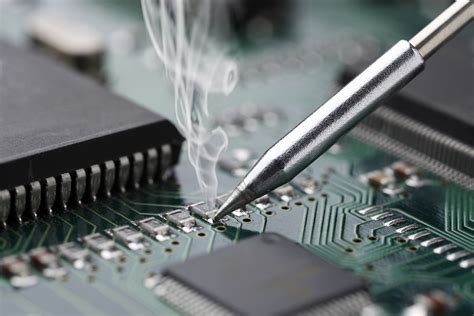
3. Reflow Soldering
After the components are placed, the populated PCB goes through a reflow soldering process. The board is heated in a reflow oven according to a precise temperature profile that meets the specifications of the solder paste and components.
The temperature profile typically ramps up gradually, has a peak temperature above the melting point of the solder, and then cools down. This melts the solder particles in the paste, forming a permanent solder joint between the component leads and PCB pads.
Some important reflow soldering parameters include:
- Preheat Temperature and Time
- Soak or Thermal Equalization
- Peak Reflow Temperature
- Time Above Liquidus (TAL)
- Cooling Rate
Proper reflow soldering forms reliable solder joints while preventing component and PCB damage from excessive heat.
4. Inspection and Quality Control
After reflow, the assembled PCBs must be inspected to verify the solder joints, component placement, and overall quality. Several inspection methods are used:
- Visual Inspection
- Automated Optical Inspection (AOI)
- X-Ray Inspection
Visual inspection is done under magnification to check for visible defects like solder bridges, insufficient solder, tombstoning, component shifting, etc. AOI uses cameras and image analysis software to rapidly check solder joints and component placement. X-ray allows seeing solder joints under components like BGAs.
Electrical testing verifies that the board operates properly:
- In-Circuit Testing (ICT)
- Flying Probe Testing
- Functional Circuit Testing
Quality control checks at multiple points in the assembly process help identify any defects or issues as early as possible.
5. Through-Hole Component Insertion
Some PCB designs use through-hole (THT) components in addition to, or instead of, surface mount parts. Through-hole component leads are inserted into holes drilled in the PCB and soldered in place. If needed, THT components are typically inserted after surface mount reflow.
THT component insertion can be done manually or with automated component insertion machines for higher volumes. Wave soldering or selective soldering processes are then used to solder the through-hole components.
6. Final Assembly and Packaging
After the PCB is fully assembled and tested, final assembly and packaging steps get it ready to ship:
- Mounting in an enclosure
- Connecting wires, cables, connectors
- Applying conformal coating for environmental protection
- Labeling and serialization
- Packaging to prevent damage in shipping
The exact final assembly steps vary widely depending on the end application and product.

PCB Assembly Methods
There are three main PCB assembly methods, each suited for different volumes and complexity:
| Assembly Method | Best Fit | Typical Volumes |
|---|---|---|
| Manual | Simple PCBs, prototypes | 1 – 100 |
| Automated SMT | Most PCBs – low to high complexity | 50 – 100,000+ |
| Automated THT | Simple to moderate THT PCBs | 100 – 10,000+ |
Manual Assembly
Manual PCB assembly is well suited for very simple PCB designs, prototypes, and very low production volumes, generally under 100 units. Operators hand solder components in place and inspect their work visually under magnification.
Manual assembly requires minimal equipment and can be done on a benchtop by a skilled operator. However, it is time consuming, prone to human error, and not practical for volume production. Quality is dependent on the skill of the individual operator.
Automated SMT Assembly
Automated surface mount technology (SMT) assembly is the most common PCB assembly method. It provides fast, precise, and repeatable results for a wide range of PCBs from simple to complex.
Automated SMT lines use programmed machines to apply solder paste, pick and place components, reflow solder, and inspect the boards. Typical inline equipment includes:
- Solder Paste Printer
- Pick and Place Machine
- Reflow Oven
- Automated Optical Inspection (AOI)
Automated SMT handles a wide range of PCB complexity and is well suited for prototype through high volume production. With some equipment, changeover between jobs can be done quickly.
Automated THT Assembly
For simple to moderately complex PCBs using mostly through-hole components, automated THT assembly may provide the best mix of speed and flexibility.
Key automated THT equipment includes:
- Wave Solder Machine
- Selective Solder Machine
Wave soldering quickly solders all THT components in one pass. For PCBs with only a few THT parts, selective soldering is faster, since each lead is soldered individually.
Automated THT is cost effective for low to moderate volumes, generally up to about 10,000 units. For high volumes and very simple THT boards, a dedicated production line may provide lower costs. However, changeover is slower compared to SMT.

PCB Assembly Design Considerations
PCB design has a big impact on the ease, speed, and quality of PCB assembly. Following PCB Assembly Guidelines helps ensure better manufacturability – known as Design for Manufacturing (DFM).
Some key PCB assembly design considerations include:
Component Selection
Using common, readily available components in standard packages simplifies sourcing and assembly. Avoid parts that are out of production or have long lead times whenever possible. Minimize the total number of unique parts.
Component Placement
Follow the component manufacturer’s guidelines for pad sizes and spacing. Place components in a grid to allow efficient routing and leave adequate space for machine pick and place. Avoid conflicts between components and tall parts that could interfere with assembly machines.
Panelization
Grouping multiple individual PCBs into a larger array or panel is an effective way to speed up assembly and reduce costs, especially for smaller boards. Determine the best panel configuration to maximize the number of boards while ensuring secure handling.
Fiducials
Add fiducial marks to the PCB to give assembly machines a reference for locating and aligning the board. Follow the equipment manufacturer’s recommendations for fiducial size, shape, and placement.
Solder Mask and Silkscreen
A clear, accurate solder mask and silkscreen help ensure proper assembly. The solder mask must match the pad sizes and spacing. Include polarity marks, component outlines, and reference designators on the silkscreen to aid in visual inspection and any hand assembly.
Taking PCB assembly into consideration during the design phase helps avoid issues that could slow down production and impact quality. Work closely with your PCB assembly partner for the best results.

PCB Assembly Services
Many companies specialize in PCB assembly services, ranging from quickturn prototypes to full production. Choosing the right partner is critical to the success of your project.
Some factors to consider when choosing a PCB assembly service include:
- Technical Capabilities
- Quality Control Systems
- Experience With Similar Projects
- Certifications (ISO, IPC, etc.)
- Turnaround Time
- Pricing
- Support and Communication
Look for a PCB assembly partner who can meet your technical requirements and has a proven track record of quality and on-time delivery. Clear communication is also essential.
Many services offer a full turnkey solution including PCB fabrication, component procurement, assembly, and testing. This can simplify your supply chain and speed up the overall process.
Frequently Asked Questions (FAQ)
What is the difference between PCB assembly and PCB fabrication?
PCB fabrication is the process of making the bare printed circuit board, while PCB assembly involves soldering components to the fabricated board. Fabrication creates the foundation, and assembly populates it with components to make it a functional circuit.
What is the difference between surface mount and through-hole assembly?
Surface mount components are soldered directly to pads on the surface of the PCB, while through-hole component leads are inserted through holes in the board and soldered on the opposite side. Surface mount is generally faster and allows smaller PCBs, but some components are only available in through-hole packages.
How much does PCB assembly cost?
PCB Assembly Costs depend on many factors including the number of components, type of components, assembly method, testing requirements, and volume. In general, larger volumes cost less per board than small quantities. Obtaining quotes from several PCB assembly services is the best way to determine the cost for a specific project.
What are the most common PCB assembly defects?
Some of the most common PCB assembly defects include:
- Solder bridges or shorts
- Insufficient or excessive solder
- Tombstoning (one end of a component lifts up)
- Component shifting or misalignment
- Incorrect component placement
- Damaged components
Proper design, process control, and inspection can minimize assembly defects.
How long does PCB assembly take?
PCB assembly time depends on the complexity of the board, the assembly method, and the current production capacity of the assembler. Simple boards using automated assembly can be completed in a few days, while complex boards or large volumes may take several weeks. Rush services are available for time-critical projects.
Conclusion
PCB assembly is a complex process that turns a bare board into a functional electronic assembly. By understanding the steps involved, the different assembly methods, and the key design considerations, you can ensure a smooth and successful project. Choosing the right PCB assembly partner is also critical. With careful planning and execution, PCB assembly brings your electronic designs to life.


Leave a Reply