What is a Prototype PCB?
A prototype printed circuit board (PCB) is the initial version of a PCB used to test and validate a new electronic circuit design before moving to high volume production. Prototype PCBs allow engineers to physically construct the circuit, program firmware, run it through various functional tests, and identify any issues or improvements needed.
Prototypes are typically made in small batches, from just 1-2 boards up to a few dozen. They closely replicate the final production intent in terms of the PCB layout, components used, assembly process, and functionality. However, some concessions may be made for prototypes, such as using a larger board size for easier probing or substituting cheaper components until the design is fully validated.
Importance of PCB Prototyping
Creating a prototype is a critical step in developing any new electronic hardware product. Prototyping allows you to:
- Test your schematic design and verify the circuit works as intended
- Write and debug firmware/software with a physical board
- Validate component selections and identify any long lead-time parts
- Optimize the PCB layout for routability, signal integrity, thermal management, etc.
- Perform early EMC/EMI testing and certifications
- Evaluate mechanical fitment in an enclosure or larger assembly
- Get feedback on the design from internal and external stakeholders
- Provide samples for demonstrations, photography, or regulatory approval
Ultimately, prototyping significantly de-risks a project by uncovering problems early in the design process when they are much easier and cheaper to fix. Diligent prototyping increases the odds that the final mass produced boards will function reliably in the end application.
PCB Prototyping Process
The basic process for creating PCB Prototypes is:
- Schematic Design – Engineer captures the circuit design in an ECAD schematic
- PCB Layout – PCB designer places components and routes traces in an ECAD layout tool
- Fabrication – Bare PCBs are manufactured by a PCB fab house
- Component Sourcing – Components are purchased from distributors or the open market
- Assembly – Components are soldered to the bare PCB by an assembly house
- Test and Rework – Assembled boards are tested and any mistakes are corrected
- Validation – Prototypes are integrated into the system and put through various functional tests
- Iterate – Design changes are made and new prototypes are built until the product is ready for production
Prototype PCB Manufacturing
Prototype PCBs are fabricated using the same processes as production boards – applying a photoresist mask, photolithography, etching away excess copper, drilling holes, plating vias, applying soldermask and silkscreen, and finally electrical test.
Where prototype fabrication differs is in the use of pooling services and rapid turn manufacturing lines. PCB pooling services aggregate many small prototype jobs onto larger panels to reduce cost. Rapid turn proto lines prioritize a quick turnaround time over absolute lowest cost.
Specs for a typical 2-layer prototype PCB might be:
| Spec | Value |
|—|—|
| Board Thickness | 1.6mm |
| Copper Weight | 1 oz outer layers |
| Soldermask | Green LPI |
| Silkscreen | White |
| Surface Finish | HASL |
| Minimum Drill | 0.3mm |
| Minimum Trace/Space | 6/6mil |
If your prototypes require more than 2 layers, tighter design rules, or advanced specs, the price and lead time will increase. Typical options for prototype fabs are:
| Service | Layers | Lead Time | Cost (qty 5) |
|---|---|---|---|
| Basic Pooling | 1-2 | 2 weeks | $50 |
| Advanced Pooling | 4-6 | 10 days | $250 |
| Quickturn Proto | 1-16 | 1-5 days | $500+ |
Prototype PCB Assembly (PCBA)
After you receive the bare fabricated boards, the next step is mounting components to create an assembled PCB. For prototypes, this is typically done by a specialized low volume assembly shop, or an in-house lab for larger companies.
Most modern prototype PCBs use surface mount components. Through-hole parts are sometimes used for large power components, connectors, or electromechanical parts like switches and relays.
The basic SMT assembly process is:
1. Apply solder paste to PCB pads via a stencil
2. Place components on the solder paste deposits
3. Reflow the board in an oven to melt the solder and create joints
4. Inspect and test the assembled board
5. Rework any missing or misaligned components
Many prototyping shops offer both automated and hand assembly services:
- Automated assembly uses a pick-and-place machine to place SMD components, screen print paste, and reflow the board
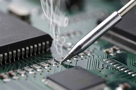
- Hand assembly uses a skilled technician with tweezers to manually place components and solder them with an iron
Automated assembly is faster and more precise for placing many small components. But for small quantities under 10 boards, the setup and stencil costs can make hand assembly more economical.
BGA components and fine pitch parts like 0402 and smaller almost always require automated assembly. Through-hole components, connectors, and mechanical parts are often hand soldered, even if the SMDs are placed by machine.
For very simple prototype boards, an engineer may be able to hand assemble it in-house. But complex designs with many small parts usually require a professional assembly shop with proper tools and trained operators.

Prototype Component Sourcing
Before you can assemble your prototypes, you need to source all the components in the Bill of Materials. Typical sources are:
- Distributors – Large catalog distributors like DigiKey, Mouser, and Arrow
- OEM/ODM – Buying directly from component manufacturers, especially for custom parts
- Brokers – Independent component brokers who locate hard to find parts
- Spot Market – Ebay, Amazon, or AliExpress often have common parts at low prices
For prototype quantities, catalog distributors are usually the most convenient option, even if they are not the cheapest. You can order cut tape quantities as low as 10pcs and receive them from in-stock in a few days.
Custom parts like the PCB, enclosure, packaging, and cable assemblies will need to be sourced from your CM or a specialized supplier. These usually have higher minimum order quantities (100-1000pcs) and lead times measured in weeks.
When planning your component sourcing for prototypes, some factors to consider are:
– Extended lead times due to supply shortages or long manufacturing cycle
– High minimum order quantities for custom, non-stocked, or niche components
– Additional cost for expedite fees, small quantity adders, and shipping fees
– Using cheaper or more available alternates for prototypes vs production
– Component shelf life and avoiding moisture sensitive parts if possible
Careful component selection and proactive sourcing can significantly speed up the prototyping process and identify any long lead time or high cost parts before production.
Testing and Validation
Once your prototypes are assembled, the next step is to power them up and ensure they function properly. For most products, the testing process looks like:
- Visual inspection – Check for any obvious assembly defects
- Smoke test – Power up the board and check that it doesn’t release any “magic smoke”
- Power test – Measure input current and verify power supplies are operating in spec
- IO test – Ensure all external interfaces like USB, Ethernet, etc. are working
- Functional test – Exercise the core application functions of the product
- Environmental test – Validate the board functions over the rated temperature, humidity, and vibration range
- EMC/EMI test – Optional pre-scans for radiated and conducted emissions
- Beta test – Let internal or external users operate the prototypes and provide feedback
Depending on the results of testing, some degree of debug and rework is usually required. This can range from simple fixes like correcting swapped components to multi-week redesigns for more complex issues.
Be prepared to spin at least 2-3 revisions of prototype boards during the validation phase. You will almost inevitably find issues and improvements as you begin integrating and testing your prototypes in the real world.
Transitioning from Prototype to Production
After your prototypes are fully tested and validated, you can prepare the design for a pilot production build. Some key steps to take are:
- Ensure your schematic and layout files are up to date with the latest prototype revisions
- Verify all components are production grade with reliable availability
- Discuss any long lead time parts with your production CM
- Get updated pricing and lead times for production quantities of the PCB and components
- Adjust your PCBA process for higher volumes, such as using a full stencil instead of dispensing paste
- Develop a comprehensive test plan and determine what level of testing will be done in production
- Plan out packaging and labeling requirements for the finished product
- Conduct a formal design review with all stakeholders to get signoff for production
Moving into production too quickly is a common mistake. It can lead to unexpected component shortages, assembly issues, or product failures in the field. Take the time to fully validate your prototypes and get all the kinks worked out before committing to a large production run.
Choosing a Prototype PCB Partner
When selecting a vendor for prototype PCBs and assembly, look for a partner that specializes in low volumes and quick-turn services. Some factors to consider are:
- PCB fabrication capabilities and lead times
- Domestic vs offshore location
- Range of components they can place (lead pitch, BGA, etc.)
- Automated vs hand assembly
- Ability to source hard to find components
- NPI process and level of engineering support
- Typical lead times and expedite options
- Pricing for your target quantity
- Quality certifications like ISO9001
- US ITAR registration if applicable
Look for reviews and recommendations from other engineers to identify shops with a proven track record. When possible, audit the facility in person to meet the team, view their equipment, and examine sample boards.
Building a strong relationship with a prototype shop pays dividends throughout the product development process. Treat your vendor as a partner and communicate your needs and expectations clearly.
PCBA Prototype Success Tips
Some final tips to aid in your PCB prototyping process:
- Start with a thorough design review before ordering boards to catch any issues early
- Use 3D models to check mechanical fit and component clearances virtually
- Communicate clearly with your fab and assembly shop about all requirements
- Consider beginning component sourcing during layout to identify any long lead time parts
- Order a few extras boards to account for assembly fallout or field failures
- Specify a comprehensive array of tests to be conducted by the assembly shop
- Don’t shortcut validation testing, especially in environmental and marginal conditions
- Incorporate feedback from all stakeholders and beta users before finalizing the design
- Stay flexible throughout the prototyping process and adapt to needed design changes
With proper planning and execution, PCB prototyping can be a smooth process that results in a robust, reliable design ready for scaling to high volume production.
FAQ
How much do PCB prototypes cost?
Prototype PCBs typically cost anywhere from $50 to $1000+ depending on the complexity of the design, layer count, quantity, and turnaround time. Simple 2-layer boards in quantities under 10 can usually be prototyped for under $250. More complex multi-layer boards with tight specs and a one week turn can cost over $1000.
How long does it take to get PCB prototypes?
Basic 2-layer PCB prototypes can usually be fabricated and shipped in 2-3 days for a premium, or 1-2 weeks with standard lead times. 4-layer and HDI prototype boards are more typically 1-2 weeks. Larger 8-16 layer boards may take 2-4 weeks depending on complexity.
What are the most common mistakes made in PCB prototyping?
Some of the most common pitfalls in PCB prototyping are:
- Failing to conduct a thorough design review before fabrication
- Not allowing sufficient time for component sourcing, especially custom or long lead time parts
- Rushing through functional validation and “real world” testing
- Not planning for respins and additional prototype iterations
- Moving to production before the design is fully proven out
Do I need to use lead-free components and assembly for prototypes?
While lead-free components and RoHS compliant assembly is not strictly required for prototypes, it is usually best to use them if possible. This avoids any surprises when transitioning to production and ensures the prototypes are fully representative. Leaded components may still be used for prototypes if they offer significant cost or availability advantages.
What is the best way to assemble my first prototype PCBs?
For most designs, using a professional prototype PCB assembly shop is the best way to assemble your first boards. They will have the equipment and expertise to reliably build and test your prototypes. Very simple designs can be hand assembled in-house if you have the tools and know-how. But complex boards with many small SMDs or BGAs usually require a professional shop.
Conclusion
PCB prototyping is a critical step in the product development process that can make or break the success of an electronics project. By partnering with an experienced PCB fab and assembly shop, carefully validating your prototypes, and staying open to design changes, you can bring a new product to market smoothly while avoiding costly mistakes. With the proper preparation and mindset, prototyping is an exciting time to see your ideas come to life and watch your product evolve into its final form.
Leave a Reply