What is PCB Warpage?
PCB warpage is the deviation of a PCB from its intended flat surface. It occurs when the board experiences uneven stress distribution, causing it to bend or twist. Warpage can happen during various stages of the PCB assembly process, including lamination, solder mask application, and reflow soldering.
Causes of PCB Warpage
1. Uneven Thermal Distribution
One of the primary causes of PCB warpage is uneven thermal distribution during the assembly process. When a PCB is exposed to high temperatures, such as during reflow soldering, different parts of the board may expand and contract at different rates. This can lead to uneven stress distribution and cause the board to warp.
Prevention Measures:
- Ensure proper preheating of the PCB before reflow soldering
- Use a consistent and controlled heating process
- Implement a gradual cooling process to minimize thermal shock
2. Incorrect Material Selection
The choice of materials used in PCB fabrication can also contribute to warpage. If the materials have different thermal expansion coefficients (CTEs), they will expand and contract at different rates when exposed to temperature changes. This can lead to uneven stress distribution and warpage.
Prevention Measures:
- Choose materials with similar CTEs
- Use high-quality, consistent materials from reliable suppliers
- Consider using low-CTE materials for critical applications
3. Improper PCB Design
Poor PCB design can also contribute to warpage. Factors such as uneven copper distribution, incorrect layer stackup, and inadequate support structures can all lead to uneven stress distribution and warpage.
Prevention Measures:
- Follow design guidelines for balanced copper distribution
- Use symmetrical layer stackups whenever possible
- Incorporate proper support structures, such as stiffeners or frames
4. Excessive Moisture Absorption
Moisture absorption can also cause PCB warpage. When a PCB absorbs moisture from the environment, it can expand and cause uneven stress distribution. This is particularly problematic during reflow soldering, as the rapid temperature change can cause the moisture to vaporize and further contribute to warpage.
Prevention Measures:
- Store PCBs in a controlled environment with low humidity
- Use moisture-barrier bags for storage and transportation
- Bake PCBs before assembly to remove excess moisture
5. Improper Handling and Storage
Improper handling and storage of PCBs can also lead to warpage. Mishandling, such as bending or twisting the board, can cause permanent deformation. Improper storage conditions, such as exposure to extreme temperatures or humidity, can also contribute to warpage.
Prevention Measures:
- Train personnel on proper handling techniques
- Use appropriate storage containers and racks
- Maintain a controlled storage environment with stable temperature and humidity

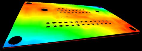
PCB Warpage Testing Methods
To ensure the quality of PCBs and minimize warpage, manufacturers can employ various testing methods. Some common testing methods include:
| Method | Description |
|---|---|
| Visual Inspection | A simple visual examination of the PCB for signs of warpage, such as bending or twisting |
| 3D Scanning | Using a 3D scanner to create a detailed digital model of the PCB, allowing for precise measurement of warpage |
| Shadow Moiré | Projecting a grid pattern onto the PCB surface and observing the distortion of the pattern to determine warpage |
| Coordinate Measuring Machine (CMM) | Using a CMM to measure the surface of the PCB at various points and compare it to the intended design |
By implementing these testing methods, manufacturers can identify warpage issues early in the assembly process and take corrective actions to minimize their impact on the final product quality.

Frequently Asked Questions (FAQ)
1. What is the acceptable level of PCB warpage?
The acceptable level of PCB warpage depends on the specific application and the components used. Generally, a warpage of less than 0.75% of the diagonal length of the board is considered acceptable for most applications. However, for high-density designs or critical applications, stricter warpage limits may be required.
2. Can PCB warpage be corrected after assembly?
In most cases, PCB warpage cannot be fully corrected after assembly. While some minor warpage may be addressed through post-assembly processes, such as baking or flattening, significant warpage will likely result in a defective product. Prevention is the best approach to minimize PCB warpage.
3. How does the reflow soldering process affect PCB warpage?
The reflow soldering process can contribute to PCB warpage due to the high temperatures involved. As the PCB is heated, different parts of the board may expand and contract at different rates, leading to uneven stress distribution and warpage. Proper control of the reflow soldering process, including preheating, consistent heating, and gradual cooling, can help minimize warpage.
4. What materials are best suited for minimizing PCB warpage?
Materials with similar thermal expansion coefficients (CTEs) are best suited for minimizing PCB warpage. Some common low-CTE materials include:
– Polyimide (PI)
– Bismaleimide Triazine (BT)
– Low-CTE FR-4
– Copper-Invar-Copper (CIC)
Using these materials in PCB fabrication can help reduce the risk of warpage due to uneven thermal expansion.
5. How can PCB design influence warpage?
PCB design plays a crucial role in minimizing warpage. Some key design considerations include:
– Balanced copper distribution: Ensuring an even distribution of copper on each layer helps minimize uneven stress distribution.
– Symmetrical layer stackup: Using a symmetrical layer stackup, with equal numbers of layers on each side of the central core, helps balance the mechanical stresses.
– Support structures: Incorporating stiffeners or frames can provide additional support and help minimize warpage.
By following these design guidelines, manufacturers can create PCBs that are more resistant to warpage and better suited for their intended applications.

Conclusion
PCB warpage is a complex issue that can have significant impacts on the quality and reliability of the final product. By understanding the top causes of warpage, such as uneven thermal distribution, incorrect material selection, improper PCB design, excessive moisture absorption, and improper handling and storage, manufacturers can take proactive steps to minimize this issue.
Implementing prevention measures, such as ensuring proper preheating, using consistent materials, following design guidelines, and maintaining a controlled storage environment, can help reduce the risk of PCB warpage. Additionally, employing various testing methods, such as visual inspection, 3D scanning, shadow moiré, and CMM, can help identify warpage issues early in the assembly process and allow for corrective actions to be taken.
By addressing PCB warpage through a combination of prevention measures and rigorous testing, manufacturers can improve the overall quality of their PCBs and ensure the reliability of their products in the field.


Leave a Reply