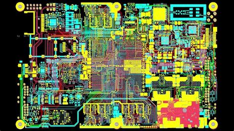
Introduction to PCB Component Placement
Proper component placement is critical when designing a printed circuit board (PCB). The location of components on the board can significantly impact the PCB’s performance, manufacturability, and reliability. This article provides a comprehensive guide to the top PCB component placement guidelines to help you optimize your circuit board designs.
Why is Proper PCB Component Placement Important?
Component placement on a PCB is important for several reasons:
-
Signal Integrity: Proper component placement helps maintain the integrity of signals traversing the board by minimizing crosstalk, electromagnetic interference (EMI), and signal reflections.
-
Thermal Management: Strategic component placement allows for efficient heat dissipation, preventing hot spots and thermal stress on the board.
-
Manufacturability: Well-planned component placement facilitates smooth assembly processes, reducing the risk of errors and improving production yields.
-
Reliability: Optimal component placement enhances the long-term reliability of the PCB by minimizing mechanical stress and ensuring proper functionality.

Key PCB Component Placement Guidelines
1. Group Related Components Together
When placing components on a PCB, it’s essential to group related components together. This practice offers several benefits:
- Shorter trace lengths between related components, reducing signal integrity issues
- Improved noise immunity due to reduced loop areas
- Simplified routing and a more organized PCB layout
Here are some examples of components that should be grouped together:
| Component Group | Examples |
|---|---|
| Power Supply | Voltage regulators, capacitors, inductors |
| Digital Logic | Microcontrollers, FPGAs, memory devices |
| Analog Circuits | Operational amplifiers, ADCs, DACs |
| RF Circuits | Antennas, filters, amplifiers |
2. Place Components for Optimal Signal Flow
When placing components on a PCB, consider the signal flow between them. Aim to place components in a logical sequence that minimizes the distance signals must travel. This approach helps reduce signal integrity issues and simplifies the routing process.
For example, in a power supply circuit, place the components in the following order:
- Input connector
- Input filter
- Rectifier
- Smoothing capacitors
- Voltage regulator
- Output capacitors
- Output connector
3. Consider Component Orientation
Component orientation plays a crucial role in PCB design. Properly orienting components can help minimize the board’s size, improve signal integrity, and facilitate efficient routing. Here are some guidelines for component orientation:
- Orient components to minimize trace lengths and crossovers
- Place tall components, such as capacitors and connectors, near the edges of the board to avoid blocking other components
- Orient IC packages with pin 1 in a consistent direction to improve readability and facilitate assembly
- Place surface-mount devices (SMDs) with their long axes parallel to the board edges to minimize tombstoning during reflow soldering
4. Minimize Crosstalk and EMI
Crosstalk and electromagnetic interference (EMI) can significantly impact a PCB’s performance. To minimize these issues, follow these guidelines:
- Separate high-speed digital traces from sensitive analog traces
- Use ground planes to provide a low-impedance return path for signals
- Implement proper grounding techniques, such as star grounding or gridded ground planes
- Place decoupling capacitors close to the power pins of ICs to reduce high-frequency noise
- Use shielding techniques, such as RF cans or shielded cables, for sensitive circuits
5. Optimize for Thermal Management
Proper thermal management is essential for ensuring the long-term reliability of a PCB. When placing components, consider the following thermal management guidelines:
- Place high-power components, such as voltage regulators or power transistors, near the edges of the board to facilitate heat dissipation
- Provide adequate spacing between high-power components to prevent thermal coupling
- Use thermal vias or heat sinks to dissipate heat from high-power components
- Orient components to allow for optimal airflow across the board
6. Consider Mechanical Constraints
When placing components on a PCB, it’s essential to consider the mechanical constraints of the enclosure or system in which the board will be used. Keep the following guidelines in mind:
- Place connectors and other mechanical components in easily accessible locations
- Ensure adequate clearance between components and the enclosure walls
- Consider the placement of mounting holes and other mechanical features
- Account for any moving parts, such as fans or actuators, and ensure they do not interfere with components
7. Follow Manufacturer’s Recommendations
Always refer to the manufacturer’s datasheets and application notes when placing components on a PCB. These resources often provide specific guidelines for component placement, such as:
- Recommended land patterns and footprints
- Minimum spacing requirements between components
- Thermal management considerations
- Specific layout recommendations for optimal performance
By following the manufacturer’s recommendations, you can ensure that your PCB design is compatible with the components you are using and minimize the risk of performance issues.

Common PCB Component Placement Mistakes to Avoid
To ensure optimal PCB performance and reliability, avoid these common component placement mistakes:
-
Placing components too close together: Inadequate spacing between components can lead to signal integrity issues, thermal problems, and manufacturing difficulties.
-
Neglecting signal integrity: Failing to consider signal integrity when placing components can result in crosstalk, EMI, and other performance issues.
-
Ignoring thermal management: Poor thermal management can lead to component overheating, reduced reliability, and premature failure.
-
Overlooking mechanical constraints: Failing to account for mechanical constraints can result in interference issues, difficulties in assembly, and reduced durability.
-
Not following manufacturer’s recommendations: Ignoring the manufacturer’s guidelines can lead to suboptimal performance and compatibility issues.

Frequently Asked Questions (FAQ)
1. What is the most important factor to consider when placing components on a PCB?
The most important factor to consider when placing components on a PCB is signal integrity. Proper component placement is crucial for maintaining the quality of signals traversing the board and minimizing issues such as crosstalk, EMI, and signal reflections.
2. How can I minimize crosstalk and EMI in my PCB design?
To minimize crosstalk and EMI in your PCB design, follow these guidelines:
- Separate high-speed digital traces from sensitive analog traces
- Use ground planes to provide a low-impedance return path for signals
- Implement proper grounding techniques, such as star grounding or gridded ground planes
- Place decoupling capacitors close to the power pins of ICs to reduce high-frequency noise
- Use shielding techniques, such as RF cans or shielded cables, for sensitive circuits
3. What are the benefits of grouping related components together on a PCB?
Grouping related components together on a PCB offers several benefits:
- Shorter trace lengths between related components, reducing signal integrity issues
- Improved noise immunity due to reduced loop areas
- Simplified routing and a more organized PCB layout
4. How can I optimize my PCB design for thermal management?
To optimize your PCB design for thermal management, consider the following guidelines:
- Place high-power components, such as voltage regulators or power transistors, near the edges of the board to facilitate heat dissipation
- Provide adequate spacing between high-power components to prevent thermal coupling
- Use thermal vias or heat sinks to dissipate heat from high-power components
- Orient components to allow for optimal airflow across the board
5. Why is it important to follow the manufacturer’s recommendations when placing components on a PCB?
Following the manufacturer’s recommendations when placing components on a PCB is important because these resources often provide specific guidelines for component placement, such as:
- Recommended land patterns and footprints
- Minimum spacing requirements between components
- Thermal management considerations
- Specific layout recommendations for optimal performance
By adhering to the manufacturer’s guidelines, you can ensure that your PCB design is compatible with the components you are using and minimize the risk of performance issues.
Conclusion
Proper component placement is a critical aspect of PCB design, impacting the board’s performance, manufacturability, and reliability. By following the top PCB component placement guidelines outlined in this article, you can optimize your circuit board designs for signal integrity, thermal management, and overall functionality.
Remember to group related components together, place components for optimal signal flow, consider component orientation, minimize crosstalk and EMI, optimize for thermal management, consider mechanical constraints, and follow the manufacturer’s recommendations.
By keeping these guidelines in mind and avoiding common placement mistakes, you can create high-quality, reliable PCBs that meet your design requirements and exceed your expectations.


Leave a Reply