Not Providing Accurate and Complete Documentation
One of the most critical aspects of placing a PCB assembly order is providing accurate and complete documentation. This includes:
- Bill of Materials (BOM)
- Gerber files
- Assembly drawings
- Component placement files
Bill of Materials (BOM)
A Bill of Materials is a comprehensive list of all the components required for your PCB assembly. It should include the following information for each component:
- Reference designator
- Manufacturer part number
- Description
- Quantity
Failing to provide a complete and accurate BOM can lead to incorrect components being used, resulting in a non-functional or subpar PCB.
Gerber Files
Gerber files are the industry standard for describing the layout of a PCB. They include information such as:
- Copper layers
- Solder mask
- Silkscreen
- Drill holes
Ensuring that your Gerber files are up-to-date and error-free is crucial for a successful PCB assembly. Common mistakes include:
- Missing layers
- Incorrect file format
- Outdated files
Assembly Drawings
Assembly drawings provide a visual representation of how components should be placed on the PCB. They should include:
- Component orientation
- Polarity indicators
- Special assembly instructions
Without clear and accurate assembly drawings, the assembly process can be prone to errors and misinterpretations.
Component Placement Files
Component placement files, also known as pick-and-place files, provide the coordinates for where each component should be placed on the PCB. They should be generated from your CAD software and include:
- Reference designator
- X and Y coordinates
- Rotation
Inaccurate or missing component placement files can lead to incorrectly placed components and a non-functional PCB.
Failing to Consider Component Availability and Lead Times
Another common mistake when placing a PCB assembly order is failing to consider component availability and lead times. This can lead to significant delays in production and increased costs.
Component Availability
Before finalizing your BOM, it’s essential to check the availability of each component. Some components may be:
- Obsolete
- On allocation
- Experiencing long lead times
By identifying potential availability issues early on, you can work with your PCB assembly partner to find suitable alternatives or plan for extended lead times.
Lead Times
Lead times can vary significantly depending on the component and supplier. Some components may be readily available, while others may have lead times of several weeks or even months.
When placing your PCB assembly order, be sure to communicate your desired timeline and work with your assembly partner to identify any potential lead time issues. This will allow you to plan accordingly and avoid delays in production.
Not Accounting for Design for Manufacturability (DFM)
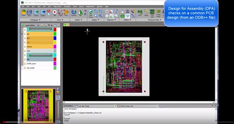
Design for Manufacturability (DFM) is the process of optimizing your PCB design to ensure efficient and cost-effective manufacturing. Failing to account for DFM can lead to a range of issues, including:
- Increased production costs
- Lower yields
- Longer manufacturing times
Some common DFM considerations include:
Minimum Trace Width and Spacing
Ensuring that your trace widths and spacing meet the capabilities of your chosen manufacturing process is crucial for a successful PCB assembly. If your traces are too narrow or too close together, it can lead to manufacturing defects and reduced yields.
Pad Size and Spacing
Similarly, pad sizes and spacing should be optimized for your chosen manufacturing process. Pads that are too small or too close together can lead to soldering difficulties and reduced reliability.
Soldermask and Silkscreen Clearance
Ensuring adequate clearance between soldermask openings and silkscreen markings is important for proper component placement and soldering. Insufficient clearance can lead to bridging and short circuits.
Via Size and Spacing
Via sizes and spacing should be optimized for your chosen manufacturing process to ensure proper plating and reliable connections between layers. Vias that are too small or too close together can lead to manufacturing defects and reduced reliability.

Ignoring PCB Surface Finish Options
The surface finish of your PCB plays a critical role in its performance, reliability, and manufacturability. Ignoring the various surface finish options available can lead to suboptimal results and increased costs.
Some common PCB surface finish options include:
- HASL (Hot Air Solder Leveling)
- ENIG (Electroless Nickel Immersion Gold)
- OSP (Organic Solderability Preservative)
- Immersion Silver
- Immersion Tin
Each surface finish has its own advantages and disadvantages, depending on the application and manufacturing process. For example:
| Surface Finish | Advantages | Disadvantages |
|---|---|---|
| HASL | – Low cost – Good solderability |
– Uneven surface – Not suitable for fine pitch |
| ENIG | – Flat surface – Excellent solderability |
– Higher cost – Potential for black pad |
| OSP | – Low cost – Flat surface |
– Limited shelf life – Not suitable for reflow |
| Immersion Silver | – Flat surface – Good solderability |
– Limited shelf life – Potential for tarnishing |
| Immersion Tin | – Flat surface – Good solderability |
– Limited shelf life – Potential for whiskers |
By considering the specific requirements of your application and working with your PCB assembly partner, you can select the optimal surface finish for your project.
Not Communicating Special Requirements or Constraints
Failing to communicate special requirements or constraints to your PCB assembly partner can lead to misunderstandings, delays, and potentially costly rework. Some examples of special requirements or constraints include:
- Controlled impedance
- High-frequency materials
- Specific component brands or traceability requirements
- Special handling or packaging requirements
- Compliance with industry standards (e.g., IPC, RoHS, UL)
By clearly communicating these requirements upfront, you can ensure that your PCB assembly partner is fully prepared to meet your needs and deliver a successful project.
Frequently Asked Questions (FAQ)
- What is the most important information to include in a Bill of Materials (BOM)?
-
The most important information to include in a BOM is the reference designator, manufacturer part number, description, and quantity for each component. Ensuring that this information is accurate and complete is crucial for a successful PCB assembly.
-
How can I avoid component availability issues when placing a PCB assembly order?
-
To avoid component availability issues, it’s important to check the availability of each component before finalizing your BOM. Work with your PCB assembly partner to identify potential issues early on and find suitable alternatives or plan for extended lead times if necessary.
-
What is Design for Manufacturability (DFM), and why is it important?
-
Design for Manufacturability (DFM) is the process of optimizing your PCB design to ensure efficient and cost-effective manufacturing. Accounting for DFM considerations such as minimum trace width and spacing, pad size and spacing, soldermask and silkscreen clearance, and via size and spacing can help reduce production costs, increase yields, and shorten manufacturing times.
-
How do I select the right surface finish for my PCB?
-
Selecting the right surface finish for your PCB depends on the specific requirements of your application and manufacturing process. Consider factors such as cost, solderability, surface flatness, and shelf life when making your decision. Work with your PCB assembly partner to determine the optimal surface finish for your project.
-
What should I do if my project has special requirements or constraints?
- If your project has special requirements or constraints, such as controlled impedance, high-frequency materials, specific component brands, or compliance with industry standards, it’s essential to communicate these clearly to your PCB assembly partner upfront. This will ensure that they are fully prepared to meet your needs and deliver a successful project.
By avoiding these common mistakes and working closely with your PCB assembly partner, you can ensure a smooth and successful PCB assembly process. Remember to provide accurate and complete documentation, consider component availability and lead times, account for Design for Manufacturability (DFM), select the appropriate surface finish, and communicate any special requirements or constraints. With these best practices in mind, you’ll be well on your way to achieving high-quality, reliable PCBs that meet your specific needs.
Leave a Reply