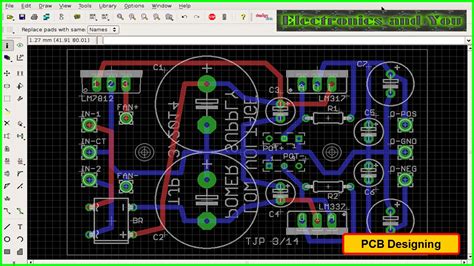
Introduction to Telecom PCB Design
Telecom PCB design is a critical aspect of the telecommunications industry, as it plays a vital role in the development of reliable and efficient communication systems. Printed Circuit Boards (PCBs) are the backbone of electronic devices, and telecom PCBs are specifically designed to meet the unique requirements of the telecommunications sector.
In this comprehensive article, we will delve into the various considerations that go into telecom PCB design, covering topics such as signal integrity, material selection, layout optimization, and manufacturing processes. By understanding these key factors, designers can create high-quality telecom PCBs that ensure optimal performance and reliability.
The Importance of Signal Integrity in Telecom PCB Design
Understanding Signal Integrity
Signal integrity is a crucial consideration in telecom PCB design, as it directly impacts the quality and reliability of the transmitted signals. Signal integrity refers to the ability of a signal to maintain its intended characteristics as it travels through the PCB and interconnects.
In the context of telecom PCBs, signal integrity is especially important due to the high-speed and high-frequency signals involved in communication systems. Ensuring proper signal integrity helps minimize signal distortion, crosstalk, and electromagnetic interference (EMI), which can degrade the overall performance of the system.
Factors Affecting Signal Integrity
Several factors can affect signal integrity in telecom PCB design, including:
-
Trace geometry: The width, spacing, and length of the traces on the PCB can impact signal integrity. Proper trace geometry is essential to maintain characteristic impedance and minimize signal reflections.
-
Dielectric materials: The choice of dielectric materials, such as FR-4 or high-frequency laminates, can influence signal propagation and loss. Materials with low dielectric constant and low loss tangent are preferred for high-speed applications.
-
Grounding and shielding: Adequate grounding and shielding techniques are necessary to minimize EMI and crosstalk between signals. Proper ground plane design and the use of shielding materials can help mitigate these issues.
-
Termination and matching: Proper termination and impedance matching techniques are essential to prevent signal reflections and ensure optimal signal transfer between components.
Techniques for Improving Signal Integrity
To address signal integrity challenges in telecom PCB design, designers can employ various techniques, such as:
-
Controlled impedance routing: Designing traces with consistent characteristic impedance helps minimize signal reflections and ensures proper signal propagation.
-
Differential signaling: Using differential pairs for high-speed signals can help cancel out common-mode noise and improve signal integrity.
-
Via optimization: Minimizing the number of vias and optimizing their placement can reduce signal discontinuities and improve signal quality.
-
Stackup design: Careful consideration of the PCB stackup, including the arrangement of signal and ground layers, can help control impedance and minimize crosstalk.
By prioritizing signal integrity in telecom PCB design, designers can ensure that the communication systems perform reliably and meet the demanding requirements of the telecommunications industry.

Material Selection for Telecom PCBs
Importance of Material Selection
The choice of materials used in telecom PCB design plays a significant role in the overall performance and reliability of the communication system. Different materials have varying electrical, thermal, and mechanical properties that can impact signal integrity, heat dissipation, and long-term durability.
When selecting materials for telecom PCBs, designers must consider factors such as dielectric constant, loss tangent, thermal conductivity, and mechanical strength. The right combination of materials can help optimize signal transmission, minimize losses, and ensure the PCB can withstand the harsh operating conditions often encountered in telecom applications.
Common Materials Used in Telecom PCBs
Some of the most commonly used materials in telecom PCB design include:
-
FR-4: FR-4 is a popular choice for general-purpose PCBs due to its low cost and good mechanical properties. However, its relatively high dielectric constant and loss tangent make it less suitable for high-frequency applications.
-
High-frequency laminates: Materials like Rogers RO4000 series, Isola IS400 series, and Taconic RF-35 are designed specifically for high-frequency applications. These laminates offer low dielectric constant, low loss tangent, and excellent thermal stability, making them ideal for telecom PCBs.
-
Copper: Copper is the most common conductor material used in PCBs due to its excellent electrical conductivity and relatively low cost. The thickness and weight of the copper foil can be adjusted based on the specific requirements of the design.
-
Solder mask: Solder mask is a protective coating applied to the PCB to prevent solder bridging and provide insulation. Choosing a high-quality solder mask with good electrical and mechanical properties is essential for telecom PCBs.
Material Properties and Their Impact on Performance
Understanding the key properties of materials and their impact on PCB performance is crucial for making informed design decisions. Some important material properties to consider include:
-
Dielectric constant (Dk): The dielectric constant measures the material’s ability to store electrical energy. A lower Dk value is preferred for high-frequency applications to minimize signal propagation delay and reduce losses.
-
Loss tangent (Df): The loss tangent represents the amount of energy lost as heat when an electrical signal passes through the material. A lower Df value is desirable to minimize signal attenuation and maintain signal integrity.
-
Thermal conductivity: Materials with high thermal conductivity can effectively dissipate heat generated by components, helping to maintain the PCB’s stability and reliability.
-
Mechanical strength: Telecom PCBs are often subjected to vibrations, shocks, and other mechanical stresses. Choosing materials with adequate mechanical strength and dimensional stability is essential to ensure the long-term reliability of the PCB.
By carefully selecting materials based on their electrical, thermal, and mechanical properties, designers can optimize the performance and reliability of telecom PCBs.

Layout Optimization for Telecom PCBs
Importance of Layout Optimization
Proper layout optimization is crucial in telecom PCB design to ensure optimal signal integrity, minimize EMI, and maximize the overall performance of the communication system. A well-optimized layout can help reduce signal losses, minimize crosstalk, and improve the manufacturability of the PCB.
When optimizing the layout of a telecom PCB, designers must consider factors such as component placement, trace routing, grounding, and shielding. By following best practices and guidelines for layout optimization, designers can create PCBs that meet the stringent requirements of the telecommunications industry.
Component Placement Considerations
Careful component placement is essential for achieving a well-optimized telecom PCB layout. Some key considerations include:
-
Signal flow: Place components in a logical sequence that follows the signal flow, minimizing the distance signals must travel and reducing the potential for signal degradation.
-
Critical components: Position critical components, such as high-speed ICs and RF modules, close to their associated components to minimize trace lengths and reduce parasitic effects.
-
Thermal management: Place heat-generating components in a way that allows for effective heat dissipation, such as near the edges of the board or in areas with good airflow.
-
Mechanical constraints: Consider the mechanical constraints of the enclosure and the placement of connectors and mounting holes when positioning components.
Trace Routing Guidelines
Proper trace routing is critical for maintaining signal integrity and minimizing EMI in telecom PCBs. Some guidelines for trace routing include:
-
Controlled impedance: Route traces with consistent characteristic impedance to minimize signal reflections and ensure proper signal propagation.
-
Trace width and spacing: Choose appropriate trace widths and spacing based on the signal’s frequency and current requirements, as well as the PCB’s manufacturing capabilities.
-
Signal layers: Use dedicated signal layers for high-speed and sensitive signals, and provide adequate ground and power planes for shielding and reference.
-
Length matching: Match the lengths of traces within a differential pair or a group of related signals to minimize skew and ensure synchronous signal arrival.
Grounding and Shielding Techniques
Effective grounding and shielding are essential for minimizing EMI and ensuring signal integrity in telecom PCBs. Some techniques to consider include:
-
Ground planes: Use solid ground planes to provide a low-impedance return path for signals and minimize EMI.
-
Grounding vias: Place grounding vias strategically to provide a low-impedance connection between ground planes and components.
-
Shielding: Use shielding techniques, such as metal enclosures or shielding cans, to isolate sensitive components and minimize external EMI.
-
Partitioning: Partition the PCB into functional blocks, each with its own local ground and power connections, to minimize crosstalk and interference between different sections of the board.
By carefully considering component placement, trace routing, grounding, and shielding during the layout optimization process, designers can create telecom PCBs that deliver optimal performance and reliability.

Manufacturing Processes for Telecom PCBs
Overview of PCB Manufacturing
The manufacturing process for telecom PCBs involves several steps that are critical to ensuring the quality and reliability of the final product. Understanding these steps and the associated best practices can help designers create PCBs that are easier to manufacture and less prone to defects.
The main steps in the PCB manufacturing process include:
-
PCB fabrication: This involves the creation of the bare PCB, including the lamination of the substrate layers, drilling of holes, and the application of copper traces and solder mask.
-
Component assembly: This step involves the placement and soldering of components onto the PCB, either through surface mount technology (SMT) or through-hole mounting.
-
Testing and inspection: The assembled PCB undergoes various tests and inspections to ensure proper functionality and adherence to quality standards.
PCB Fabrication Techniques
Several PCB fabrication techniques are commonly used in the manufacturing of telecom PCBs, including:
-
Multilayer PCBs: Telecom PCBs often require multiple layers to accommodate the high density of components and signals. Multilayer PCBs are fabricated by laminating several layers of substrate material together, with copper traces and vias connecting the layers.
-
High-density interconnect (HDI): HDI PCBs use advanced fabrication techniques, such as microvias and fine-pitch traces, to achieve higher component density and improved signal integrity.
-
Controlled impedance: Fabricating PCBs with controlled impedance requires precise control over the dimensions and spacing of the traces, as well as the dielectric properties of the substrate material.
-
Surface finish: The choice of surface finish, such as hot air solder leveling (HASL), immersion silver, or electroless nickel immersion gold (ENIG), can impact the solderability and long-term reliability of the PCB.
Component Assembly Methods
Two primary methods are used for assembling components onto telecom PCBs:
-
Surface mount technology (SMT): SMT involves placing components directly onto the surface of the PCB and soldering them in place using reflow soldering. SMT allows for higher component density and faster assembly compared to through-hole mounting.
-
Through-hole mounting: Through-hole mounting involves inserting component leads through holes drilled in the PCB and soldering them on the opposite side. While less common than SMT, through-hole mounting is still used for certain components, such as connectors and large power devices.
Testing and Quality Control
Thorough testing and quality control are essential to ensure that telecom PCBs meet the required performance and reliability standards. Some common testing methods include:
-
In-circuit testing (ICT): ICT involves using a bed-of-nails fixture to test the PCB for shorts, opens, and component values.
-
Functional testing: Functional testing verifies that the assembled PCB performs as intended, often using custom test fixtures and software.
-
Boundary scan testing: Boundary scan testing, also known as JTAG testing, uses a built-in test infrastructure to test the interconnections between components on the PCB.
-
X-ray inspection: X-ray inspection is used to detect hidden defects, such as voids in solder joints or misaligned components, that may not be visible through visual inspection.
By understanding the manufacturing processes and best practices associated with telecom PCBs, designers can create designs that are optimized for manufacturability, ensuring high-quality and reliable products.
Frequently Asked Questions (FAQ)
- What are the key considerations for choosing materials for telecom PCBs?
When selecting materials for telecom PCBs, designers should consider factors such as dielectric constant, loss tangent, thermal conductivity, and mechanical strength. The choice of materials can significantly impact signal integrity, heat dissipation, and long-term reliability. High-frequency laminates with low dielectric constant and loss tangent are often preferred for telecom applications.
- Why is signal integrity important in telecom PCB design?
Signal integrity is crucial in telecom PCB design because it directly affects the quality and reliability of the transmitted signals. Poor signal integrity can lead to signal distortion, crosstalk, and electromagnetic interference (EMI), which can degrade the overall performance of the communication system. Ensuring proper signal integrity helps maintain the intended signal characteristics and minimizes signal degradation.
- What are some techniques for improving signal integrity in telecom PCBs?
Designers can employ various techniques to improve signal integrity in telecom PCBs, such as:
– Controlled impedance routing: Designing traces with consistent characteristic impedance to minimize signal reflections.
– Differential signaling: Using differential pairs for high-speed signals to cancel out common-mode noise.
– Via optimization: Minimizing the number of vias and optimizing their placement to reduce signal discontinuities.
– Stackup design: Carefully arranging signal and ground layers to control impedance and minimize crosstalk.
- What are the main steps in the manufacturing process for telecom PCBs?
The main steps in the manufacturing process for telecom PCBs include:
1. PCB fabrication: Creating the bare PCB by laminating substrate layers, drilling holes, and applying copper traces and solder mask.
2. Component assembly: Placing and soldering components onto the PCB using surface mount technology (SMT) or through-hole mounting.
3. Testing and inspection: Conducting various tests and inspections to ensure proper functionality and adherence to quality standards.
- How can designers optimize the layout of telecom PCBs?
To optimize the layout of telecom PCBs, designers should consider factors such as:
– Component placement: Placing components in a logical sequence that follows the signal flow, minimizing trace lengths, and considering thermal management and mechanical constraints.
– Trace routing: Using controlled impedance routing, choosing appropriate trace widths and spacing, using dedicated signal layers, and matching trace lengths within differential pairs or related signals.
– Grounding and shielding: Employing solid ground planes, strategic grounding vias, shielding techniques, and partitioning the PCB into functional blocks to minimize EMI and ensure signal integrity.
By understanding and addressing these key aspects of telecom PCB design, manufacturers can create high-quality, reliable PCBs that meet the demanding requirements of the telecommunications industry.
Conclusion
Telecom PCB design is a complex and challenging field that requires careful consideration of various factors to ensure optimal performance and reliability. By understanding the importance of signal integrity, selecting appropriate materials, optimizing layouts, and adhering to best practices in manufacturing, designers can create telecom PCBs that meet the stringent requirements of the telecommunications industry.
This comprehensive article has explored the key aspects of telecom PCB design, including signal integrity, material selection, layout optimization, and manufacturing processes. By delving into each of these topics and providing practical insights and guidelines, we aim to equip designers with the knowledge and tools necessary to create high-quality telecom PCBs.
As the telecommunications industry continues to evolve and demand ever-higher levels of performance and reliability, staying up-to-date with the latest design considerations and best practices is essential. By continuously learning and adapting to new challenges, designers can push the boundaries of what is possible in telecom PCB design and contribute to the advancement of the industry as a whole.


Leave a Reply