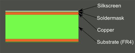
What is PCB Silkscreen?
PCB silkscreen, also known as legend printing or screen printing, is a method of applying text, logos, and other markings onto the surface of a printed circuit board (PCB). The process involves using a fine mesh screen to transfer ink onto the PCB, creating a durable and legible marking that helps with component identification, assembly, and troubleshooting.
The Silkscreen Process
The silkscreen process consists of several steps:
-
Design: The desired markings are designed using CAD software, ensuring that the text and graphics are clear and properly sized for the PCB.
-
Screen Preparation: A fine mesh screen is coated with a light-sensitive emulsion, and the design is transferred onto the screen using a photographic process.
-
Ink Application: The screen is placed over the PCB, and ink is applied using a squeegee, forcing it through the open areas of the screen and onto the PCB surface.
-
Curing: The ink is then cured using heat or UV light, depending on the type of ink used, to ensure a strong bond and durability.
The Importance of PCB Silkscreen
1. Component Identification
One of the primary purposes of PCB silkscreen is to clearly label components on the board. This includes:
- Component reference designators (e.g., R1, C2, U3)
- Component values (e.g., 10k, 22µF, 74HC00)
- Polarity markings (e.g., + and – for capacitors and diodes)
Having these markings on the PCB makes it easier for technicians and engineers to identify components during assembly, testing, and troubleshooting.
2. Assembly Guidelines
PCB silkscreen can also provide important guidelines for the assembly process, such as:
- Component orientation (e.g., indicating the direction of a diode or IC)
- Placement outlines (e.g., showing the correct position for a component)
- Warning symbols (e.g., indicating high-voltage areas or sensitive components)
These markings help ensure that components are placed correctly during manual or automated assembly, reducing the risk of errors and improving overall quality.
3. Branding and Aesthetics
Silkscreen can be used to apply company logos, product names, and other branding elements to the PCB. This helps to create a professional appearance and can be important for product recognition and marketing. Additionally, a well-designed silkscreen layout can enhance the overall aesthetics of the PCB, making it more visually appealing.
4. Regulatory Compliance
In some cases, PCB silkscreen is used to apply regulatory markings and certifications, such as:
- UL (Underwriters Laboratories) certification marks
- CE (Conformité Européenne) marking
- RoHS (Restriction of Hazardous Substances) compliance symbols
These markings are important for demonstrating compliance with industry standards and regulations, which is often required for products to be sold in certain markets.
5. Revision Tracking
PCB silkscreen can include revision numbers or date codes, allowing for easy tracking of board versions and manufacturing dates. This information is valuable for quality control, troubleshooting, and product lifecycle management.

Silkscreen Design Considerations
When designing PCB silkscreen, several factors should be considered to ensure optimal readability and durability:
1. Font Size and Style
The font size and style used for silkscreen text should be chosen carefully to ensure legibility. Minimum font sizes typically range from 0.8mm to 1.5mm, depending on the application and the capabilities of the silkscreen process. Sans-serif fonts are often preferred for their clarity and simplicity.
2. Line Width
The line width of silkscreen graphics should be wide enough to be clearly visible but not so thick that it obscures underlying features or pads. A minimum line width of 0.15mm to 0.2mm is common, although this may vary depending on the specific silkscreen process and ink used.
3. Spacing
Adequate spacing should be maintained between silkscreen elements and other features on the PCB, such as component pads, vias, and traces. A minimum clearance of 0.2mm to 0.5mm is typically recommended to avoid interference and ensure legibility.
4. Color
White is the most common color for PCB silkscreen, as it provides good contrast against the typical green or black solder mask. However, other colors, such as yellow or black, may be used for specific applications or to enhance contrast on different solder mask colors.
5. Placement
Silkscreen elements should be placed in a way that minimizes interference with other PCB features and allows for easy reading during assembly and troubleshooting. This may involve orienting text to be read from a specific direction or placing markings in areas that are not obscured by components.

Frequently Asked Questions (FAQ)
1. Is silkscreen necessary for all PCBs?
While silkscreen is highly beneficial for most PCBs, it is not always necessary. Some simple or low-cost boards may omit silkscreen to reduce production costs, while others may rely on alternative markings, such as direct legend printing or laser-marked labels.
2. Can silkscreen be applied to both sides of a PCB?
Yes, silkscreen can be applied to both the top and bottom sides of a PCB. This is often done to provide assembly information or branding on both sides of the board.
3. How durable is PCB silkscreen?
PCB silkscreen is generally very durable and can withstand normal handling and exposure to various environmental conditions. However, excessive abrasion or exposure to harsh chemicals may cause the markings to fade or wear off over time.
4. Can silkscreen be used on flexible PCBs?
Yes, silkscreen can be applied to flexible PCBs, although the process may require special considerations, such as the use of flexible inks and adjusted curing methods to ensure proper adhesion and durability.
5. Are there any limitations to the complexity of silkscreen designs?
While silkscreen is capable of producing detailed graphics and text, there are some limitations to the complexity of designs that can be achieved. Very fine details or intricate logos may be difficult to reproduce accurately, and the specific capabilities will depend on the silkscreen process and equipment used.

Conclusion
PCB silkscreen is a crucial aspect of PCB fabrication, providing a range of benefits that enhance the functionality, usability, and appearance of printed circuit boards. From component identification and assembly guidelines to branding and regulatory compliance, silkscreen markings play a vital role in ensuring the quality and reliability of electronic products.
By understanding the importance of PCB silkscreen and considering key design factors, such as font size, line width, spacing, color, and placement, PCB designers can create boards that are both functional and visually appealing. As the electronics industry continues to evolve, the use of silkscreen will remain an essential tool for producing high-quality, user-friendly PCBs.
| Aspect | Recommendation |
|---|---|
| Font Size | 0.8mm – 1.5mm |
| Line Width | 0.15mm – 0.2mm |
| Spacing | 0.2mm – 0.5mm clearance |
| Color | White (most common) |
| Placement | Minimize interference, orient for easy reading |
Table 1: PCB Silkscreen Design Recommendations
By following these guidelines and working closely with experienced PCB manufacturers, designers can ensure that their PCBs are equipped with clear, durable, and informative silkscreen markings that contribute to the overall success of their electronic products.


Leave a Reply