Step 1: Design and Fabrication of PCB
The first step in PCB Assembly is the design and fabrication of the PCB. The design process involves creating a schematic diagram and a layout of the PCB using specialized software. The schematic diagram shows the electrical connections between the components, while the layout shows the physical placement of the components on the PCB.
Once the design is complete, the PCB is fabricated using a process called photolithography. This involves applying a photoresist layer to a copper-clad board, exposing it to UV light through a mask, and then etching away the unwanted copper to leave the desired circuit pattern.
Step 2: Solder Paste Application
The second step in PCB assembly is the application of solder paste to the PCB. Solder paste is a mixture of tiny solder particles suspended in flux. It is applied to the PCB using a stencil or a screen printing process.
The stencil is a thin metal sheet with holes that correspond to the pads on the PCB. The solder paste is squeezed through the holes onto the pads using a squeegee. The screen printing process involves using a mesh screen with a pattern that corresponds to the pads on the PCB. The solder paste is pushed through the screen onto the pads using a squeegee.

Step 3: Component Placement
The third step in PCB assembly is the placement of the electronic components onto the PCB. This is done using a pick-and-place machine, which is an automated system that picks up the components from a feeder and places them onto the PCB with high precision.
The pick-and-place machine uses a vacuum nozzle to pick up the components and a camera to align them with the pads on the PCB. The machine can place components at a rate of several thousand per hour, depending on the complexity of the PCB and the number of components.

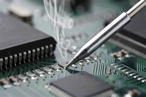
Step 4: Reflow Soldering
The fourth step in PCB assembly is reflow soldering. This involves heating the PCB and the components to a high temperature to melt the solder paste and form a permanent connection between the components and the PCB.
The reflow soldering process is done in a reflow oven, which has several heating zones that gradually increase the temperature of the PCB and the components. The temperature profile of the reflow oven is carefully controlled to ensure that the solder melts and flows properly without damaging the components or the PCB.

Step 5: Inspection and Testing
The fifth step in PCB assembly is inspection and testing. This involves visually inspecting the PCB for any defects or errors in the soldering process, such as bridging, insufficient solder, or misaligned components.
In addition to visual inspection, the PCB may also undergo functional testing to ensure that it is working properly. This may involve using specialized test equipment to measure the electrical properties of the PCB and the components, such as resistance, capacitance, and voltage.
Step 6: Conformal Coating
The sixth step in PCB assembly is conformal coating. This involves applying a thin layer of protective coating to the PCB to protect it from moisture, dust, and other environmental factors that can affect its performance and reliability.
There are several types of conformal coatings, including acrylic, silicone, and urethane. The choice of coating depends on the specific requirements of the PCB, such as its operating environment, temperature range, and level of protection needed.
Step 7: Final Assembly and Packaging
The final step in PCB assembly is final assembly and packaging. This involves attaching any additional components, such as connectors, switches, or displays, to the PCB and then packaging it for shipment or installation into the final product.
The packaging process may involve placing the PCB into a protective case or enclosure, adding any necessary labels or markings, and then sealing the package to prevent damage during transportation or storage.
Advantages of PCB Assembly
PCB assembly offers several advantages over other methods of electronic circuit construction, such as point-to-point wiring or wire wrapping. Some of the key advantages include:
Compact Size
PCBs allow for a high density of components to be mounted on a small surface area, which results in a compact and lightweight final product. This is especially important for applications where space is limited, such as in mobile devices or wearable electronics.
Reliability
PCBs are highly reliable due to the use of automated assembly processes and rigorous testing procedures. The soldered connections between the components and the PCB are strong and durable, and the protective coatings help to prevent damage from environmental factors.
Cost-Effective
PCB assembly is a cost-effective method of electronic circuit construction, especially for high-volume production runs. The automated assembly processes and standardized components help to reduce labor costs and minimize errors, while the compact size of the PCB reduces material costs.
Flexibility
PCBs can be designed and customized to meet the specific requirements of a wide range of applications, from simple single-layer boards to complex multi-layer boards with high-speed digital signals and power electronics.
Challenges of PCB Assembly
While PCB assembly offers many advantages, there are also several challenges that must be addressed to ensure a successful outcome. Some of the key challenges include:
Component Availability
The availability of electronic components can be a challenge, especially for newer or specialized components. Lead times for some components can be long, and shortages can occur due to high demand or supply chain disruptions.
Soldering Defects
Soldering defects, such as bridging, insufficient solder, or cold solder joints, can occur during the assembly process and can lead to reliability issues or performance problems. Proper process control and inspection procedures are essential to minimize these defects.
Thermal Management
PCBs generate heat during operation, and proper thermal management is essential to ensure reliable performance and longevity. This may involve the use of heat sinks, fans, or other cooling techniques to dissipate heat from the components and the PCB.
Electromagnetic Interference
PCBs can generate electromagnetic interference (EMI) that can affect the performance of other electronic devices or cause regulatory compliance issues. Proper design techniques, such as shielding, grounding, and filtering, can help to minimize EMI and ensure compliance with regulatory standards.
Conclusion
PCB assembly is a complex process that involves several steps, from design and fabrication to final assembly and packaging. By following these steps and addressing the key challenges, manufacturers can ensure a high-quality and reliable final product that meets the specific requirements of the application.
As electronic devices continue to become smaller, faster, and more complex, the importance of PCB assembly will only continue to grow. By staying up-to-date with the latest technologies and best practices, manufacturers can stay competitive and deliver innovative products to their customers.
Frequently Asked Questions (FAQ)
What is PCB assembly?
PCB assembly is the process of mounting electronic components onto a printed circuit board (PCB) to create a functional electronic circuit. It involves several steps, including design, fabrication, solder paste application, component placement, reflow soldering, inspection, and testing.
What are the advantages of PCB assembly?
PCB assembly offers several advantages over other methods of electronic circuit construction, including compact size, reliability, cost-effectiveness, and flexibility. PCBs allow for a high density of components to be mounted on a small surface area, resulting in a compact and lightweight final product. The automated assembly processes and rigorous testing procedures ensure high reliability, while the standardized components and compact size help to reduce costs.
What are the challenges of PCB assembly?
Some of the key challenges of PCB assembly include component availability, soldering defects, thermal management, and electromagnetic interference. Component availability can be a challenge, especially for newer or specialized components, while soldering defects can lead to reliability issues or performance problems. Proper thermal management is essential to ensure reliable performance and longevity, while electromagnetic interference can affect the performance of other electronic devices or cause regulatory compliance issues.
What is reflow soldering?
Reflow soldering is a process used in PCB assembly to melt the solder paste and form a permanent connection between the electronic components and the PCB. It involves heating the PCB and the components to a high temperature in a reflow oven, which has several heating zones that gradually increase the temperature. The temperature profile of the reflow oven is carefully controlled to ensure that the solder melts and flows properly without damaging the components or the PCB.
What is conformal coating?
Conformal coating is a thin layer of protective coating applied to the PCB to protect it from moisture, dust, and other environmental factors that can affect its performance and reliability. There are several types of conformal coatings, including acrylic, silicone, and urethane, and the choice of coating depends on the specific requirements of the PCB, such as its operating environment, temperature range, and level of protection needed.


Leave a Reply