Introduction to PCB Plating
PCB plating is a crucial process in the manufacturing of printed circuit boards (PCBs). It involves the deposition of a thin layer of metal onto the surface of the PCB to enhance its electrical conductivity, durability, and solderability. Plating is essential for ensuring reliable electrical connections between components and protecting the PCB from environmental factors such as oxidation and corrosion.
Types of PCB Plating
There are several types of PCB plating, each with its own unique properties and applications. The most common types of PCB plating include:
-
Copper Plating: Copper is the most widely used material for PCB plating due to its excellent electrical conductivity and low cost. It is typically applied as a base layer before other types of plating.
-
Tin Plating: Tin plating is often used as a protective layer over copper to prevent oxidation and improve solderability. It is also used as a final finish for some PCBs.
-
Nickel Plating: Nickel plating is used as a barrier layer between copper and other types of plating, such as gold or silver. It provides excellent corrosion resistance and helps to prevent the diffusion of copper into the final finish.
-
Gold Plating: Gold plating is used in high-reliability applications where superior electrical conductivity and corrosion resistance are required. It is often used in connectors, switches, and other critical components.
-
Silver Plating: Silver plating is sometimes used as an alternative to gold plating due to its lower cost and similar electrical properties. However, it is less commonly used due to its tendency to tarnish over time.
The Importance of Hole Plating in PCBs
Hole plating, also known as through-hole plating, is a specific type of PCB plating that involves depositing a layer of metal inside the drilled holes of a PCB. This process is crucial for creating reliable electrical connections between the different layers of a multi-layer PCB.
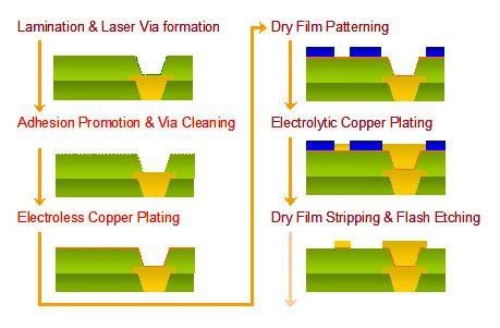
The Hole Plating Process
The hole plating process typically involves the following steps:
-
Drilling: Holes are drilled into the PCB using a CNC machine or laser drilling system.
-
Desmearing: The drilled holes are cleaned and the resin smear is removed using a chemical or plasma desmearing process.
-
Electroless Copper Deposition: A thin layer of copper is deposited onto the walls of the drilled holes using an electroless plating process. This layer acts as a conductive seed layer for the subsequent electroplating process.
-
Electroplating: The PCB is immersed in an electrolytic bath containing the desired plating metal (usually copper). An electric current is applied, causing the metal ions to be attracted to the surface of the PCB and deposited onto the walls of the drilled holes.
-
Inspection: The plated holes are inspected for quality and conformance to specifications using automated optical inspection (AOI) systems or manual visual inspection.
Benefits of Hole Plating
Hole plating offers several key benefits in PCB manufacturing:
-
Reliable Electrical Connections: Hole plating ensures that electrical signals can pass reliably between the different layers of a multi-layer PCB.
-
Mechanical Strength: Plated holes provide additional mechanical strength to the PCB, helping to prevent delamination and other structural failures.
-
Improved Thermal Management: Plated holes can help to dissipate heat more effectively, which is particularly important in high-power applications.
-
Enhanced Manufacturability: Hole plating allows for the use of smaller vias and more complex PCB designs, improving overall manufacturability.

Factors Affecting PCB Plating Quality
Several factors can impact the quality of PCB plating, including:
-
Surface Preparation: Proper surface preparation is essential for ensuring good adhesion between the plating metal and the PCB substrate. This includes cleaning, etching, and activation of the surface prior to plating.
-
Plating Bath Composition: The composition of the plating bath, including the concentration of metal ions, pH, and temperature, must be carefully controlled to ensure consistent and high-quality plating.
-
Current Density: The current density used during electroplating can affect the uniformity and grain structure of the deposited metal layer. Higher current densities generally result in faster plating rates but may lead to increased stress and reduced adhesion.
-
Plating Thickness: The thickness of the plated layer must be carefully controlled to ensure adequate conductivity and protection while minimizing cost and maintaining compatibility with downstream processes such as soldering.
-
Contamination: Contamination of the plating bath or PCB surface can lead to defects such as nodules, pits, and voids in the plated layer. Careful process control and regular maintenance are necessary to minimize contamination.

Advanced PCB Plating Techniques
In addition to traditional PCB plating methods, there are several advanced techniques that offer improved performance and functionality:
Selective Plating
Selective plating involves the targeted deposition of plating metal onto specific areas of the PCB, rather than the entire surface. This technique can be used to create local regions with enhanced electrical or mechanical properties, such as increased thickness or hardness. Selective plating is often used in applications such as edge connector fingers and press-fit pins.
Immersion Plating
Immersion plating is a simple and cost-effective method for depositing thin layers of metal onto a PCB surface. In this process, the PCB is immersed in a plating solution containing the desired metal ions, which are then reduced and deposited onto the surface through a chemical reaction. Immersion plating is commonly used for applying final finishes such as silver or tin.
Electrochemical Pattern Plating (ECPP)
Electrochemical pattern plating is a specialized technique for selectively plating fine-pitch patterns onto a PCB surface. In this process, a patterned photoresist layer is applied to the PCB, exposing only the areas to be plated. The PCB is then immersed in an electrolytic bath and an electric current is applied, causing the metal to be deposited onto the exposed areas. ECPP is often used for creating high-density interconnects and fine-pitch structures.

Quality Control and Inspection of PCB Plating
Ensuring the quality and consistency of PCB plating is critical for maintaining the reliability and performance of the finished product. Several methods are used for quality control and inspection of plated PCBs:
-
Visual Inspection: Manual visual inspection is often used to identify gross defects such as nodules, pits, and voids in the plated layer.
-
Automated Optical Inspection (AOI): AOI systems use high-resolution cameras and image processing algorithms to automatically detect and classify plating defects.
-
Cross-Sectional Analysis: Destructive cross-sectional analysis can be used to evaluate the thickness, uniformity, and adhesion of the plated layer.
-
Electrical Testing: Electrical testing, such as continuity and resistance measurements, can be used to verify the functionality and reliability of plated interconnects.
-
Accelerated Life Testing: Accelerated life testing, such as thermal cycling and humidity exposure, can be used to evaluate the long-term reliability of plated PCBs under simulated environmental conditions.
Environmental and Safety Considerations in PCB Plating
PCB plating involves the use of chemicals and processes that can have significant environmental and safety impacts. It is important for PCB manufacturers to implement appropriate controls and best practices to minimize these risks:
-
Wastewater Treatment: Plating processes generate significant volumes of wastewater containing heavy metals and other pollutants. Proper treatment and disposal of this wastewater is essential for protecting the environment and complying with regulations.
-
Air Emissions: Some plating processes, such as electroless plating, can generate air emissions containing volatile organic compounds (VOCs) and other pollutants. Appropriate ventilation and emission control systems must be used to minimize these emissions.
-
Chemical Safety: Many of the chemicals used in PCB plating, such as acids and cyanides, are hazardous to human health and the environment. Proper handling, storage, and disposal of these chemicals is critical for ensuring worker safety and preventing accidental releases.
-
Personal Protective Equipment (PPE): Workers involved in PCB plating must be provided with appropriate PPE, such as gloves, goggles, and respirators, to protect against exposure to hazardous chemicals and fumes.
-
Environmental Management Systems: PCB manufacturers should implement formal environmental management systems, such as ISO 14001, to systematically identify, control, and improve their environmental performance.
Frequently Asked Questions (FAQ)
-
What is the difference between electroplating and electroless plating?
Electroplating involves the use of an external electrical current to deposit metal ions onto the surface of the PCB, while electroless plating relies on a chemical reaction to reduce and deposit the metal ions without the use of an external current. -
What is the purpose of applying a soldermask over the plated PCB surface?
The soldermask is a protective layer that is applied over the plated PCB surface to prevent solder bridging and accidental short circuits during the assembly process. It also provides insulation and protection against environmental factors such as moisture and abrasion. -
Can PCBs be re-plated if the original plating is damaged or worn?
In some cases, PCBs can be stripped of their original plating and re-plated with new metal layers. However, this process can be challenging and may not be cost-effective for all applications. It is generally preferable to prevent plating damage through proper design, handling, and maintenance. -
What are some common defects that can occur in PCB plating?
Common defects in PCB plating include nodules, pits, voids, cracks, and delamination. These defects can be caused by a variety of factors, such as improper surface preparation, contamination, incorrect plating parameters, or mechanical stress. -
How can PCB designers optimize their designs for better plating performance?
PCB designers can optimize their designs for better plating performance by following guidelines such as maintaining appropriate trace widths and spacings, avoiding sharp corners and acute angles, and providing adequate clearance around plated holes and vias. They should also consider the specific requirements and limitations of the intended plating process and collaborate closely with the PCB manufacturer to ensure optimal results.
Conclusion
PCB plating and hole plating are critical processes in the manufacturing of high-quality and reliable printed circuit boards. By understanding the types of plating available, the factors affecting plating quality, and the advanced techniques and quality control methods used in the industry, PCB designers and manufacturers can optimize their processes to achieve the best possible results.
However, it is also important to recognize the environmental and safety impacts of PCB plating and to implement appropriate controls and best practices to minimize these risks. By adopting a holistic approach that balances technical performance, cost-effectiveness, and environmental responsibility, the PCB industry can continue to innovate and grow while contributing to a more sustainable future.


Leave a Reply