Understanding the PCB Fabrication Process
The Basics of PCB Manufacturing
PCB fabrication involves a series of steps that transform a design into a functional printed circuit board. The process begins with the creation of a PCB design using specialized software, such as Altium Designer or Eagle. The design is then transferred to a copper-clad laminate substrate, which forms the base of the PCB.
Etching and Plating
Once the design is transferred to the substrate, the unwanted copper is removed through a process called etching. This leaves behind the desired copper traces that will carry electrical signals. The board then undergoes a plating process, where additional copper is deposited onto the traces to increase their thickness and improve their current-carrying capacity.
Drilling and Layering
After etching and plating, holes are drilled into the board to accommodate through-hole components and provide interconnections between layers. Multi-layer PCBs are fabricated by stacking and laminating several single-layer boards together, with insulating material between each layer.
Solder Mask and Silkscreen
A solder mask, typically green in color, is applied to the PCB to protect the copper traces from oxidation and prevent accidental short circuits during soldering. A silkscreen layer is then added to provide text and symbols for component placement and identification.
Materials Used in PCB Fabrication
Substrate Materials
The most common substrate material used in PCB fabrication is FR-4, a glass-reinforced epoxy laminate. FR-4 offers excellent electrical insulation, mechanical strength, and thermal stability. Other substrate materials include:
- Polyimide: Used for high-temperature applications
- Teflon: Offers superior dielectric properties
- Aluminum: Provides excellent thermal dissipation
Copper Foil
Copper foil is the conductive material used for creating traces on the PCB. It is available in various thicknesses, typically measured in ounces per square foot (oz/ft²). Common thicknesses include:
| Thickness (oz/ft²) | Thickness (µm) |
|---|---|
| 0.5 | 17.5 |
| 1 | 35 |
| 2 | 70 |
Solder Mask and Silkscreen Inks
Solder mask and silkscreen inks are essential for protecting the PCB and providing clear markings. Solder mask inks are typically epoxy-based and are available in various colors, with green being the most common. Silkscreen inks are usually white or yellow and are formulated to adhere well to the solder mask.

PCB Design Considerations for Fast and Quality Fabrication
Design for Manufacturability (DFM)
To ensure fast and quality PCB fabrication, it is crucial to consider Design for Manufacturability (DFM) principles. DFM involves designing a PCB that is easy to manufacture, assemble, and test. Some key DFM guidelines include:
- Maintaining proper trace width and spacing
- Avoiding acute angles in traces
- Providing sufficient clearance around holes and components
- Using standardized component sizes and footprints
Signal Integrity and EMI Reduction
Signal integrity and electromagnetic interference (EMI) reduction are critical factors in PCB design. To maintain signal integrity and minimize EMI, designers should:
- Use appropriate trace widths and lengths
- Implement proper grounding and shielding techniques
- Utilize differential signaling for high-speed data transmission
- Incorporate filters and suppression components
Thermal Management
Effective thermal management is essential for ensuring the reliability and longevity of electronic components. PCB designers should consider the following:
- Placing high-heat components away from sensitive devices
- Incorporating thermal vias and heat sinks
- Using thermally conductive substrate materials
- Providing adequate ventilation and cooling solutions

Quality Control in PCB Fabrication
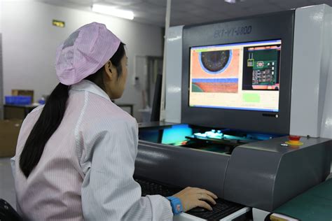
Automated Optical Inspection (AOI)
Automated Optical Inspection (AOI) is a computer-based system that uses high-resolution cameras and image processing software to detect manufacturing defects on PCBs. AOI systems can identify issues such as:
- Missing or misaligned components
- Solder bridging or insufficient solder
- Incorrect component polarity
- Trace and pad defects
In-Circuit Testing (ICT)
In-Circuit Testing (ICT) is a method of verifying the functionality of individual components and their interconnections on a PCB. ICT systems use a bed-of-nails fixture to make contact with test points on the board, allowing for the measurement of:
- Component values (resistors, capacitors, inductors)
- Diode and transistor functionality
- Short circuits and open connections
Functional Testing
Functional testing involves verifying the overall performance of the assembLED PCB in its intended application. This type of testing ensures that the PCB meets the specified requirements and operates correctly under various conditions, such as:
- Different voltage and current levels
- Temperature variations
- Vibration and shock
- Electromagnetic compatibility (EMC)

Choosing a PCB Fabrication Partner
Quality Standards and Certifications
When selecting a PCB fabrication partner, it is essential to consider their quality standards and certifications. Some important certifications to look for include:
- ISO 9001: Quality Management Systems
- IPC-A-600: Acceptability of Printed Boards
- UL 94: Standard for Safety of Flammability of Plastic Materials
- RoHS: Restriction of Hazardous Substances
Lead Times and Pricing
Fast PCB fabrication is crucial for meeting tight project deadlines. When evaluating potential fabrication partners, consider their lead times and pricing structure. Many PCB Manufacturers offer expedited services for an additional cost, allowing you to receive your boards faster when needed.
Technical Support and Communication
Effective communication and technical support are key to a successful PCB fabrication partnership. Look for a manufacturer that provides clear and responsive communication channels, such as email, phone, or online chat. Additionally, consider their ability to offer technical guidance and support throughout the fabrication process.
Frequently Asked Questions (FAQ)
-
What is the difference between single-layer and multi-layer PCBs?
Single-Layer PCBs have conductive traces on only one side of the substrate, while multi-layer PCBs have traces on both sides and additional internal layers. Multi-layer PCBs offer higher component density and better signal integrity but are more complex and costly to manufacture. -
What is the minimum trace width and spacing for PCB fabrication?
The minimum trace width and spacing depend on the PCB manufacturer’s capabilities and the specific design requirements. Typically, a minimum trace width of 0.006 inches (0.15 mm) and a minimum spacing of 0.006 inches (0.15 mm) are achievable by most manufacturers. -
How long does it take to fabricate a PCB?
PCB fabrication lead times vary depending on the complexity of the design, the chosen manufacturer, and the selected service level. Standard lead times can range from 5 to 15 business days, while expedited services can reduce the lead time to 1-5 business days. -
What is the difference between hard gold and soft gold plating?
Hard gold plating is typically used for edge connectors and high-wear areas on a PCB, as it offers better durability and wear resistance. Soft gold plating is more commonly used for Wire Bonding and surface mount pads, as it provides better solderability and wire bond adhesion. -
Can I combine different surface finishes on the same PCB?
Yes, it is possible to have different surface finishes on the same PCB. This is called a mixed-finish PCB and is often used when certain components require specific finishes for optimal performance or compatibility. However, mixed-finish PCBs may have higher fabrication costs and longer lead times.
In conclusion, fast and quality PCB fabrication is essential for the success of electronic products in today’s competitive market. By understanding the fabrication process, materials, design considerations, and quality control measures, engineers and product developers can ensure that their PCBs are manufactured to the highest standards. Partnering with a reliable and experienced PCB fabrication company is crucial for achieving the best results in terms of speed, quality, and cost-effectiveness.


Leave a Reply