Introduction to PCB Testing
Printed Circuit Boards (PCBs) are essential components in virtually all modern electronic devices. They provide the foundation upon which electronic components are mounted and interconnected to form functional circuits. The reliability and performance of these devices heavily depend on the quality of the PCBs. To ensure that PCBs meet the required standards and function as intended, thorough testing is crucial throughout the manufacturing process.
PCB testing involves various methods and techniques to verify the integrity of the board, its components, and the interconnections. Among these methods, functional testing plays a vital role in validating the performance of the assembled PCB under real-world operating conditions. This article will delve into the importance of functional testing in PCB manufacturing, its types, procedures, and best practices.
The Importance of PCB Testing
PCB testing is an integral part of the manufacturing process for several reasons:
-
Quality Assurance: Testing ensures that the manufactured PCBs meet the specified quality standards and are free from defects that could compromise their functionality or reliability.
-
Cost Savings: Identifying and rectifying issues early in the manufacturing process can significantly reduce the cost of rework and prevent the release of defective products into the market.
-
Reliability: Thorough testing helps identify potential failure points and weaknesses in the PCB design, allowing for improvements that enhance the overall reliability of the final product.
-
Compliance: Many industries have specific regulations and standards that PCBs must adhere to. Testing ensures that the boards comply with these requirements.

Types of PCB Testing
There are several types of PCB testing, each focusing on different aspects of the board’s functionality and quality. Some of the common types include:
-
Visual Inspection: This involves manually inspecting the PCB for any visible defects, such as incorrect component placement, solder bridges, or damaged traces.
-
Automated Optical Inspection (AOI): AOI uses high-resolution cameras and image processing software to automatically detect surface-level defects on the PCB.
-
X-Ray Inspection: This non-destructive testing method uses X-rays to examine the internal structure of the PCB, including solder joints and component placement.
-
In-Circuit Testing (ICT): ICT involves using a bed-of-nails fixture to make electrical contact with specific points on the PCB and test the functionality of individual components and their interconnections.
-
Flying Probe Testing: This method utilizes movable probes to make electrical contact with test points on the PCB, allowing for more flexibility compared to ICT.
-
Boundary Scan Testing: Also known as JTAG testing, this method uses built-in test circuitry to verify the functionality of digital components and their interconnections.
-
Functional Testing: This type of testing focuses on validating the overall functionality of the assembled PCB under real-world operating conditions.

Functional Testing in PCB Manufacturing
Functional testing is a crucial step in PCB manufacturing that ensures the assembled board performs as intended in its final application. It involves subjecting the PCB to various stimuli and verifying its response against the expected behavior.
Objectives of Functional Testing
The primary objectives of functional testing in PCB manufacturing include:
-
Verifying Functionality: Ensure that the assembled PCB functions as per the design specifications and requirements.
-
Identifying Defects: Detect any defects or issues that may have gone unnoticed during previous testing stages.
-
Validating Performance: Assess the PCB’s performance under different operating conditions, such as varying temperatures, voltages, and frequencies.
-
Ensuring Compatibility: Verify that the PCB is compatible with other components or systems it will interact with in the final application.
Functional Testing Procedures
Functional testing typically involves the following procedures:
-
Test Planning: Develop a comprehensive test plan that outlines the test objectives, methods, and acceptance criteria based on the PCB’s design specifications and requirements.
-
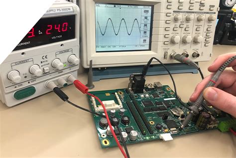
Test Setup: Prepare the necessary test equipment, such as power supplies, signal generators, oscilloscopes, and custom test fixtures, as per the test plan.
-
Test Execution: Apply the specified stimuli to the PCB and measure its response using the appropriate test equipment. This may involve powering up the board, applying input signals, and monitoring output signals.
-
Results Analysis: Compare the measured results against the expected values and determine whether the PCB meets the acceptance criteria. Document any deviations or failures for further investigation and corrective action.
Best Practices for Functional Testing
To ensure effective and efficient functional testing, consider the following best practices:
-
Early Involvement: Engage the testing team early in the PCB design process to identify potential testability issues and incorporate necessary test points or features.
-
Comprehensive Test Coverage: Develop test cases that cover all the critical functions and operating conditions of the PCB, including edge cases and stress tests.
-
Automated Testing: Utilize automated test equipment (ATE) and software to streamline the testing process, reduce human error, and improve repeatability.
-
Test Fixture Design: Design custom test fixtures that provide reliable and consistent electrical contact with the PCB’s test points, minimizing the risk of false failures.
-
Traceability: Maintain detailed records of the test results, including any failures, corrective actions, and retests, to ensure traceability and accountability.

Case Studies
Case Study 1: Automotive ECU Functional Testing
An automotive electronics manufacturer implemented functional testing for their engine control units (ECUs). The test setup included a hardware-in-the-loop (HIL) simulator that emulated various engine sensors and actuators. The functional test cases covered different engine operating conditions, such as starting, idling, acceleration, and deceleration. The test results helped identify issues related to sensor signal processing and fuel injection timing, which were rectified before the ECUs were released for production.
Case Study 2: Medical Device PCB Functional Testing
A medical device company developed a portable patient monitor that required rigorous functional testing to ensure reliability and safety. The test plan included verifying the functionality of the device’s sensors, display, alarms, and data communication interfaces. The testing team used a combination of automated test scripts and manual test cases to validate the device’s performance under various scenarios, such as low battery conditions, sensor disconnections, and data corruption. The functional testing helped uncover a critical issue related to the device’s alarm system, which was addressed through a firmware update.
Challenges and Solutions
Functional testing in PCB manufacturing can present several challenges, such as:
-
Complexity: As PCBs become more complex with increased functionality and miniaturization, designing comprehensive test cases and fixtures becomes more challenging.
-
Time and Cost: Functional testing can be time-consuming and expensive, especially for high-volume production runs or complex boards with numerous test points.
-
Testability: Some PCB designs may lack sufficient test points or access to critical signals, making functional testing difficult or impossible.
To overcome these challenges, consider the following solutions:
-
Design for Testability (DFT): Collaborate with the PCB design team to incorporate testability features, such as test points, boundary scan cells, and built-in self-test (BIST) circuits.
-
Modular Testing: Break down the functional testing into smaller, manageable modules that can be tested independently, reducing the overall testing time and complexity.
-
Automated Test Equipment (ATE): Invest in ATE that can handle high-volume testing and provide accurate and repeatable results, reducing the reliance on manual testing.
-
Simulation and Emulation: Use simulation and emulation tools to validate the PCB’s functionality before the physical prototypes are available, allowing for early detection and correction of design issues.
Frequently Asked Questions (FAQ)
-
What is the difference between functional testing and in-circuit testing?
Functional testing focuses on validating the overall functionality of the assembled PCB under real-world operating conditions, while in-circuit testing verifies the functionality of individual components and their interconnections using a bed-of-nails fixture. -
How do I determine the appropriate functional test coverage for my PCB?
The appropriate functional test coverage depends on the PCB’s complexity, criticality, and the requirements of the end application. Consider factors such as the number of functions, operating conditions, and potential failure modes when developing the test plan. -
Can functional testing replace other types of PCB testing?
While functional testing is an essential part of PCB testing, it should not be considered a replacement for other types of testing, such as visual inspection, AOI, or ICT. Each testing method focuses on different aspects of the PCB’s quality and should be used in combination for comprehensive coverage. -
How can I reduce the time and cost of functional testing?
To reduce the time and cost of functional testing, consider implementing automation, modular testing, and design for testability (DFT) practices. Collaborate with the PCB design team to incorporate testability features and optimize the test strategy early in the development process. -
What should I do if a PCB fails functional testing?
If a PCB fails functional testing, document the failure details, including the test case, conditions, and observed behavior. Investigate the root cause of the failure, which may involve additional testing, visual inspection, or design review. Implement the necessary corrective actions, such as component replacement, rework, or design changes, and retest the PCB to ensure the issue has been resolved.
Conclusion
Functional testing is a critical aspect of PCB manufacturing that ensures the assembled board performs as intended in its final application. By subjecting the PCB to various stimuli and verifying its response against the expected behavior, functional testing helps identify defects, validate performance, and ensure compatibility. Implementing best practices, such as early involvement, comprehensive test coverage, and automation, can significantly enhance the effectiveness and efficiency of functional testing.
As PCBs continue to evolve in complexity and functionality, the importance of thorough and reliable functional testing will only grow. By understanding the objectives, procedures, and challenges associated with functional testing, PCB manufacturers can develop robust testing strategies that guarantee the quality and reliability of their products.
Glossary
- AOI: Automated Optical Inspection
- ATE: Automated Test Equipment
- BIST: Built-In Self-Test
- DFT: Design for Testability
- ECU: Electronic Control Unit
- HIL: Hardware-in-the-Loop
- ICT: In-Circuit Testing
- JTAG: Joint Test Action Group (Boundary Scan Testing)
- PCB: Printed Circuit Board
| Term | Definition |
|---|---|
| AOI | Automated Optical Inspection |
| ATE | Automated Test Equipment |
| BIST | Built-In Self-Test |
| DFT | Design for Testability |
| ECU | Electronic Control Unit |
| HIL | Hardware-in-the-Loop |
| ICT | In-Circuit Testing |
| JTAG | Joint Test Action Group (Boundary Scan Testing) |
| PCB | Printed Circuit Board |
By embracing functional testing as an integral part of the PCB manufacturing process, manufacturers can deliver high-quality, reliable products that meet the ever-increasing demands of the electronics industry. With the right approach and tools, functional testing can be a powerful ally in the pursuit of PCB excellence.


Leave a Reply