Introduction to Image Transfer in PCB Manufacturing
Image transfer is a critical step in the printed circuit board (PCB) manufacturing process. It involves transferring the designed circuit pattern onto the copper-clad laminate or PCB substrate. The accuracy and precision of the image transfer process directly impact the quality and functionality of the final PCB product.
In this article, we will dive deep into the image transfer process, exploring various methods, their advantages and disadvantages, and the latest advancements in the field.
Understanding the PCB Manufacturing Process
Before we delve into the specifics of image transfer, let’s briefly overview the PCB manufacturing process to understand where image transfer fits in.
-
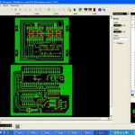
PCB Design: The process begins with designing the circuit using specialized PCB design software. The design includes the layout of components, traces, and other features.
-
Printing the Circuit Pattern: The designed circuit pattern is printed onto a transparent film or photomask. This film will be used in the image transfer process.
-
Image Transfer: The printed circuit pattern is transferred onto the copper-clad laminate or PCB substrate using one of the image transfer methods discussed later in this article.
-
Etching: After image transfer, the unwanted copper is etched away, leaving behind the desired circuit pattern.
-
Drilling: Holes are drilled into the PCB for component placement and vias.
-
Surface Finishing: The PCB undergoes surface finishing to protect the exposed copper and enhance solderability.
-
Solder Mask Application: A solder mask is applied to the PCB to insulate and protect the copper traces.
-
Silkscreen Printing: The component labels and other markings are printed onto the PCB using silkscreen printing.
-
Assembly and Testing: The PCB is populated with components, soldered, and tested for functionality.
Image Transfer Methods
There are several methods used for image transfer in PCB manufacturing, each with its own advantages and limitations. Let’s explore the most common methods:
1. Photolithography
Photolithography, also known as optical lithography, is the most widely used image transfer method in PCB manufacturing. It involves the following steps:
- The copper-clad laminate is coated with a light-sensitive photoresist.
- The photomask with the circuit pattern is placed on top of the photoresist-coated laminate.
- The laminate is exposed to ultraviolet (UV) light, which passes through the transparent areas of the photomask and hardens the photoresist in those areas.
- The unexposed photoresist is removed using a developer solution, leaving behind the hardened photoresist in the desired circuit pattern.
Advantages of photolithography:
– High resolution and accuracy
– Suitable for high-volume production
– Well-established and widely used method
Disadvantages of photolithography:
– Requires a clean room environment
– Involves the use of chemicals
– Higher setup costs compared to other methods
2. Screen Printing
Screen printing is a cost-effective image transfer method suitable for low-volume production or prototype PCBs. The process involves the following steps:
- A fine mesh screen is coated with a light-sensitive emulsion.
- The circuit pattern is transferred onto the screen using a photomask and exposure to UV light.
- The unexposed emulsion is washed away, creating openings in the screen for the circuit pattern.
- The screen is placed on top of the copper-clad laminate, and conductive ink is forced through the openings onto the laminate using a squeegee.
- The ink is cured using heat or UV light to form the circuit pattern.
Advantages of screen printing:
– Low setup costs
– Suitable for low-volume production and prototyping
– Faster turnaround times compared to photolithography
Disadvantages of screen printing:
– Lower resolution and accuracy compared to photolithography
– Limited to simpler circuit designs
– Ink compatibility issues with certain surface finishes
3. Inkjet Printing
Inkjet printing is a digital image transfer method that has gained popularity in recent years. It offers a flexible and cost-effective solution for low-volume production and rapid prototyping. The process involves the following steps:
- The circuit pattern is designed using specialized software.
- A digital inkjet printer is used to dispense conductive ink directly onto the copper-clad laminate or PCB substrate.
- The ink is cured using heat or UV light to form the circuit pattern.
Advantages of inkjet printing:
– No need for photomasks or screens
– Quick turnaround times
– Suitable for low-volume production and prototyping
– Allows for easy design changes and customization
Disadvantages of inkjet printing:
– Lower resolution compared to photolithography
– Limited material compatibility
– Requires specialized inkjet printers and inks
4. Laser Direct Imaging (LDI)
Laser direct imaging (LDI) is a advanced image transfer method that uses a laser to directly expose the photoresist-coated laminate. The process involves the following steps:
- The copper-clad laminate is coated with a light-sensitive photoresist.
- A laser beam is used to selectively expose the photoresist in the desired circuit pattern.
- The unexposed photoresist is removed using a developer solution, leaving behind the hardened photoresist in the circuit pattern.
Advantages of LDI:
– High resolution and accuracy
– Eliminates the need for photomasks
– Allows for quick design changes
– Suitable for high-volume production
Disadvantages of LDI:
– High equipment costs
– Requires specialized laser equipment and software
– Limited material compatibility

Factors Affecting Image Transfer Quality
Several factors can impact the quality of the image transfer process in PCB manufacturing. These include:
-
Photomask Quality: The quality of the photomask directly affects the accuracy and resolution of the transferred circuit pattern. Photomasks must be free from defects and have high optical density.
-
Laminate Surface Preparation: The copper-clad laminate surface must be clean, smooth, and free from contaminants to ensure proper adhesion of the photoresist or ink.
-
Exposure Parameters: Proper exposure time, intensity, and wavelength are crucial for achieving optimal results in photolithography and LDI processes.
-
Developer and Etchant Chemistry: The chemistry and concentration of the developer and etchant solutions must be carefully controlled to ensure accurate pattern transfer and minimize undercutting.
-
Environmental Conditions: Temperature, humidity, and air quality can affect the performance of the photoresist, ink, and other materials used in the image transfer process.
Advancements in Image Transfer Technology
Image transfer technology continues to evolve, driven by the demand for higher resolution, improved accuracy, and faster turnaround times. Some of the latest advancements in the field include:
-
Direct Imaging (DI): Direct imaging systems use high-resolution digital imaging to directly expose the photoresist without the need for photomasks. This technology offers improved accuracy, faster setup times, and the ability to handle complex designs.
-
Nanoimprint Lithography: Nanoimprint lithography is an emerging technology that uses a mold to transfer the circuit pattern onto the laminate. It offers high resolution and has the potential to replace photolithography in certain applications.
-
Conductive Inkjet Printing: The development of advanced conductive inks has enabled the use of inkjet printing for creating conductive traces and components directly on the PCB substrate. This technology offers new possibilities for printed electronics and flexible circuits.
Image Transfer and PCB Quality Control
Image transfer is a critical step in PCB manufacturing, and ensuring its quality is essential for producing reliable and high-performance PCBs. Quality control measures are implemented throughout the image transfer process to identify and address any issues.
Some common quality control techniques include:
-
Visual Inspection: Visual inspection is performed to identify any defects, such as incomplete transfer, overexposure, or underexposure, in the transferred circuit pattern.
-
Automated Optical Inspection (AOI): AOI systems use cameras and image processing algorithms to automatically detect and classify defects in the transferred circuit pattern.
-
Electrical Testing: Electrical testing is performed to verify the continuity and insulation resistance of the transferred circuit pattern. This helps identify any short circuits or open circuits caused by defects in the image transfer process.
-
Microsectioning: Microsectioning involves cross-sectioning the PCB and examining the transferred circuit pattern under a microscope to assess the quality and accuracy of the image transfer process.
By implementing thorough quality control measures, PCB manufacturers can identify and address image transfer issues early in the manufacturing process, reducing the risk of defects and ensuring the production of high-quality PCBs.
Conclusion
Image transfer is a vital step in the PCB manufacturing process, directly impacting the quality and functionality of the final product. Understanding the various image transfer methods, their advantages and limitations, and the factors affecting image transfer quality is crucial for PCB designers and manufacturers.
As technology continues to advance, new image transfer methods and materials are being developed to meet the ever-increasing demands for higher resolution, improved accuracy, and faster turnaround times. By staying up-to-date with the latest advancements and implementing robust quality control measures, PCB manufacturers can ensure the production of high-quality, reliable PCBs that meet the needs of today’s electronic devices.
Frequently Asked Questions (FAQ)
-
What is the most common image transfer method used in PCB manufacturing?
The most common image transfer method used in PCB manufacturing is photolithography, also known as optical lithography. It involves using a photomask and light-sensitive photoresist to transfer the circuit pattern onto the copper-clad laminate. -
What are the advantages of inkjet printing for image transfer in PCB manufacturing?
Inkjet printing offers several advantages for image transfer in PCB manufacturing, including no need for photomasks or screens, quick turnaround times, suitability for low-volume production and prototyping, and the ability to easily make design changes and customizations. -
How does laser direct imaging (LDI) differ from traditional photolithography?
Laser direct imaging (LDI) differs from traditional photolithography in that it uses a laser to directly expose the photoresist-coated laminate, eliminating the need for photomasks. LDI offers high resolution and accuracy, allows for quick design changes, and is suitable for high-volume production. -
What factors can affect the quality of the image transfer process in PCB manufacturing?
Several factors can affect the quality of the image transfer process in PCB manufacturing, including photomask quality, laminate surface preparation, exposure parameters, developer and etchant chemistry, and environmental conditions such as temperature, humidity, and air quality. -
What quality control measures are used to ensure the accuracy and reliability of the image transfer process?
Quality control measures used to ensure the accuracy and reliability of the image transfer process include visual inspection, automated optical inspection (AOI), electrical testing, and microsectioning. These techniques help identify and address any defects or issues in the transferred circuit pattern, ensuring the production of high-quality PCBs.
Leave a Reply